An introduction to FPGA power
February 19, 2015

Designing the power system for a field-programmable gate array (FPGA) is no easy task. FPGAs are highly configurable semiconductor devices that are us...
Designing the power system for a field-programmable gate array (FPGA) is no easy task. FPGAs are highly configurable semiconductor devices that are used in an array of applications and end markets. Common examples include communications, automotive, industrial, medical, video, and defense. Since they’re highly configurable, various components can be placed around them to form the final system design. Although the list of potential applications and systems can be endless, a common denominator in all designs is that they all need power.
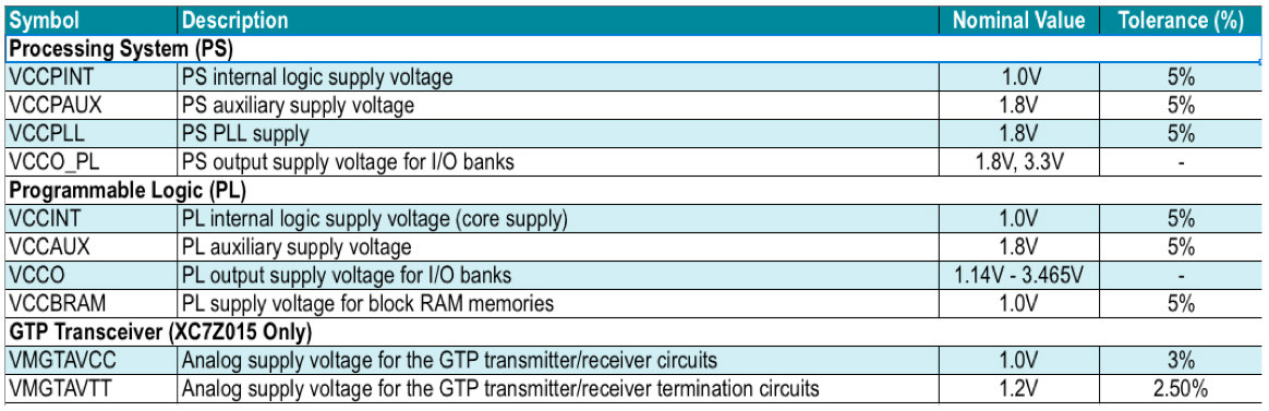
Several voltage rails are typically required to power up an FPGA. Depending on your application, your primary input supply may originate from a backplane, isolated supply, non-isolated supply, or even a battery. From these primary inputs, an intermediate DC voltage is typically generated to power the FPGA’s main rails. These intermediate voltages are typically 5 V or 12 V DC. Some typical rails, voltages, and tolerances FPGAs are listed in Tables 1 and 2.
|
|

|
|
Determining the appropriate current levels for each rail can be a tricky task as currents can range from a couple hundred milliamps to 60 A and above. Planning ahead can make all the difference to avoid the mistakes of either overdesigning (paying too much) or under designing (having to redesign) your power rails. FPGA vendors offer accurate tools to estimate your worst-case power consumption based on how you’ll be utilizing the FPGA.
The Xilinx Power Estimator (XPE), shown in Figure 1, covers several families of Xilinx FPGAs. Within the tool, you can select the exact part you’re using and input your clock and configuration information to determine your power supply needs and make the appropriate device selection based on the estimates.
|
|

Design considerations
Many factors must be considered when choosing a proper power supply to fit an FPGA application. Cost, size, and efficiency are always a consideration when designing any power supply, but in FPGA applications, some rails will have different requirements than others. Core rails usually need to maintain tighter accuracy over line, load, and temperature. Some rails, such as transceivers, are more sensitive to noise and need to maintain their output below a certain noise threshold. Other things to consider are that some rails with common voltages may be combined and can be isolated with a ferrite bead for filtering or a load switch.
When designing to meet the tolerance requirement, consider all fixed and dynamic operating conditions. First, choose a regulator with less than a 1 percent reference accuracy, which leaves you with the most room for design margin to handle the dynamic operating conditions like load transients.
High-speed transceiver rails also must be designed with caution since noise on these sensitive rails can degrade performance and increase jitter. Low-dropout regulators (LDOs) are a good choice for these rails. But when higher currents are necessary, switching supplies can be used as long as the output ripple typically remains below 10 mVpk-pk over the 10 kHz to 80 MHz frequency range. Your specific FPGA datasheet will contain detailed specs on the transceiver requirements.
Power supply sequencing is another important aspect to consider when designing an FPGA power design. Since several rails provide power to a FPGA, following the recommended power sequence achieves the minimum current drawn at startup, which in turn prevents damage to your device. The recommended power-up supply sequence for both the logic and transceiver supply rails on the Virtex 7 series FPGA is shown in Figure 2. Processor sequencing for the Zynq 7000 series SoC is pictured in Figure 3.
|
|

|
|

These rails must have a monotonic rise and must all be powered on in a period ranging from 0.2 ms to 50 ms for Xilinx 7/Zynq 7000 series families and 0.2 to 40 ms for Xilinx Ultrascale FPGA family. The recommended power-down sequence is the reverse order of the power-up sequence.
Power solutions
Once the appropriate current levels have been estimated and all design considerations known, power supply designers can begin device selection. Several options are available, such as LDOs, SMPS, and integrated modules, with each offering some tradeoffs. For example, LDOs are a good choice to power some lower current FPGA rails because of their simplicity and low output noise. The drawback to LDOs is that they can be inefficient and dissipate a lot of heat through the pass transistor at higher currents. They’re typically good for low-power applications and those that require low noise.
When more than a couple of amps are needed and efficiency is more critical, designers can turn to a switch-mode power supply (SMPS). These devices can approach greater than 90 percent efficiency and provide up to 30 A in a single-phase configuration. They require more design effort compared to an LDO and may not be as efficient at lighter loads, but offer benefits include flexibility and efficiency at higher current levels.
Power modules, such as the LMZ31506 simple switcher, can integrate a DC/DC converter, power MOSFETs, a shielded inductor, and passives into a low-profile QFN package. This can reduce design time since everything is already integrated into one package and only minimal external components are needed.
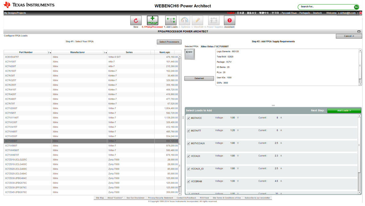
Webench FPGA architect
Webench FPGA Architect (Figure 4) is a useful tool that helps a power supply designer construct several FPGA power rails within minutes. The tool incorporates some of the detailed supply requirements of the latest available FPGAs. Once within the tool, you simply select the exact FPGA you’re using and adjusting your current levels as necessary and the tool will assemble a comprehensive design report.
|
|