
Why You Should Consider .8mm PCBs Versus 1.6mm
April 12, 2024
Blog
Printed circuit boards, i.e. PCBs, are often manufactured using an FR4 (fire retardant fiberglass) substrate, with a final thickness of 1.6mm. However, PCBs don’t have to be 1.6mm. Another common size is .8mm.
In this article, I’ll outline advantages and disadvantages of both 1.6mm and .8mm boards (in the context of a 2-layer PCB) and discuss if you should use a .8mm PCB instead of 1.6mm in your design.
Cost and Fulfillment (~Advantage .8mm)
As the de facto PCB standard, 1.6mm boards tend to be quite reasonably priced. At the same time, .8mm PCBs are half the volume of their 1.6 mm counterparts, bringing numerous benefits for PCB manufacturers in terms of materials and warehousing costs. As such, the cost of either tends to be similar, though not always the same.
Considering a generic order of (100) 100 x 100mm boards, PCBWay’s online quoting system output the following prices:
- 1.6mm – PCB Cost $135.87, DHL Shipping $49.55
- .8mm – PCB Cost $125.41, DHL Shipping $35
OSHPark Lists:
- 1.6mm PCBs $5 per square inch (1oz copper)
- .8mm PCBs $5 per square inch (2oz copper)
So, you may save money using a .8mm PCB, however, fulfillment is typically slower for .8mm boards when compared to 1.6mm. OSHPARK ships 1.6mm PCBs in 9-12 days versus 12-21 days for .8mm PCBs. PCBWay lists a 3-4 day build time for 1.6mm boards, versus 4-5 days for .8mm PCBs as of this writing.
Weight and Volume (Advantage .8mm)

Caption: They have to be stored somewhere! / Image Credit: Jeremy Cook
Perhaps the most obvious advantage of .8mm PCBs is that their weight and volume is roughly half that of a 1.6mm PCB per surface area. Volume and weight contribute to shipping costs, thus the difference seen in PCBWay’s fulfillment prices. While perhaps not a huge deal for 100 boards, if you ramp up to 1000, 10,000, or more, costs can be significant. Once in-house you must then warehouse boards (volume), and ship to customers for another potentially weight and volume-dependent charge.
You should also consider the weight of the end-product and how this affects something’s performance. While a single lighter PCB might not make a huge difference to a finished automobile, consider how 100 similar changes across a design might affect it. In other situations, e.g. a smartwatch or drone, the PCB itself may be a sizable percentage of the device’s weight and volume that needs to be minimized. Here .8mm PCBs may present significant advantages.
Crosstalk and Characteristic Impedance (Advantage .8mm)
Consider that in a 2-layer PCB, the thinner the board, the closer the two copper sides are to each other, and the more effectively a bottom ground layer can minimize crosstalk on an opposite signal layer. As a .8mm PCB is nominally half the thickness of a 1.6mm board, this distance effect is significant. This can also affect the characteristic impedance between signal lines, but how this impacts your overall design will depend on the situation.
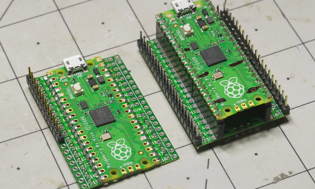
An example of this opposite layer ground effect is found in Raspberry Pi’s RP2040 design guide, section 2.4.1, in the context of USB signal transmission. The board discussed there is actually 1mm in thickness, but the guide notes that one would need to reconsider how the D+ and D- USB connections are designed if a (thicker) 1.6mm board was instead used.
Mechanical Pros/Cons (Advantage 1.6mm)

Image Credit: Jeremy Cook
As seen in the image above, it is quite easy to bend the .8mm prototype Pico Touch 2 board featured here. Going through my scrap PCBs, a 1.6mm board of roughly the same size is very difficult to bend. That prototype board was designed with a rat bite separation pattern, which was pretty easy to break apart in its .8mm format. Of course, you can do the same sort of separation with a 1.6mm board, even if it may be a little harder. So, I wouldn’t consider it a make or break proposition.
However, mechanical factors can be important:
- If you are making your PCB a structural element, e.g. a drone body, the part’s rigidity (versus its weight) should be seriously considered. The greater the surface area, the more potential for deformation.
- Conversely, there are niche applications where you may want a PCB to flex, such as my LED/battery holder PCB.
- Solder fatigue can cause a design to fail, as repeated deformations can cause stress on solder joints. One would normally see this as an advantage for more rigid 1.6mm boards, however, a .8mm PCB’s increased flexibility could serve to soften impacts. The details of your situation must be considered and analyzed individually.
- .8mm boards tend to flex more during assembly, potentially causing issues.
Specific Form Factors (Varies)
When working with specific hardware, a specification will often dictate the need to use a certain thickness PCB. M.2 connectors, for instance, require a .8mm PCB and you may find this specified elsewhere in your technological explorations. While this choice might be obvious, don’t forget to check the spec… and check the .8mm box when ordering. I suspect you wouldn’t be the first person to neglect this essential step.
Is .8mm the Solution for You?
In summary, if you need a low-cost, low-weight, and low-volume two-layer board, and need to deal with potential crosstalk issues, consider a .8mm PCB for your application. At the same time, if you need excellent mechanical strength and potentially faster fulfillment, then 1.6mm may be the better choice. Of course, for specific form-factors, e.g. M.2, then the choice may already be made for you.
Whatever your project needs, we live in an amazing time considering the range of resources available to us in the form of quick-turn PCB vendors, software, and even information available to us. For more ideas, join me for the Developing With Arduino instructional series each month this year (2024), where I talk about using the Arduino ecosystem in the professional world.


