
Single-core, low-footprint NB-IoT design challenges
January 25, 2017
While the traditional mobile operators industry has focused on high end, high throughput application for the booming smartphone market, it's accumulat...
While the traditional mobile operators industry has focused on high end, high throughput application for the booming smartphone market, it’s accumulated delays in standardization of a technology, which allows long range, low cost, and a massive number of low power devices in the operator-licensed spectrum. Competing technologies, such as LoRA, Sigfox, and others, have been successful in filling this gap, and the threat these are posing have hugely accelerated the push for a 3GPP standard that would counteract these competitive forces. As a result of this push and relevant 3GPP work items, Cat-0 and Cat-M standards were published in 2014 and 2016 to address some of the challenges, allowing, for example, a 75 percent reduction of complexity and much better power consumption techniques to address the IoT requirement of many years of battery operation without memory intervention.
It became clear, however, that a clean slate approach was necessary to address the specific IoT segment where only small, occasional bursts of data are sent and received by a massive number of devices with maximum spectrum efficiency and the highest coverage. Following a big industry debate about the technology impact on existing networks and LTE compatibility, a narrowband IoT (NB-IoT) standard (or Cat-NB1) was published in June 2016. The new standard allows for more than 200,000 devices in a cell, and coverage has been improved by 20 dB compared to general packet radio service (GPRS) reference, allowing low-power battery-operated devices to be reached, for instance, in a remote basement or behind walls.
Challenges of protocol stacks implementation in ultra-low power, low-cost devices
In the system-on-chip (SoC) design for NB-IoT (and cellular IoT in general, including Cat-M1), design efforts need to be directed at optimizing power and cost rather than optimizing performance as in previous SoC design for the mobile industry.
Regarding protocol stack design, the following considerations need to be part of initial design:
Memory footprint
An optimized program memory footprint is of great importance in IoT design, as this allows the SoC to run the software directly from embedded flash memory rather than from external flash, allowing savings in both cost and power consumption.
The optimization of the RAM usage is even more important, as RAM will be embedded in the SoC. To this point, the design for the protocol stack needs to be done from scratch rather than downscaled from an existing LTE legacy design. Careful configurability of the various optional features like non-IP, IP, control, or user plane optimization, compressions etc., also allow the protocol stack to be tailored to the operator and OEM requirements with optimal memory usage.
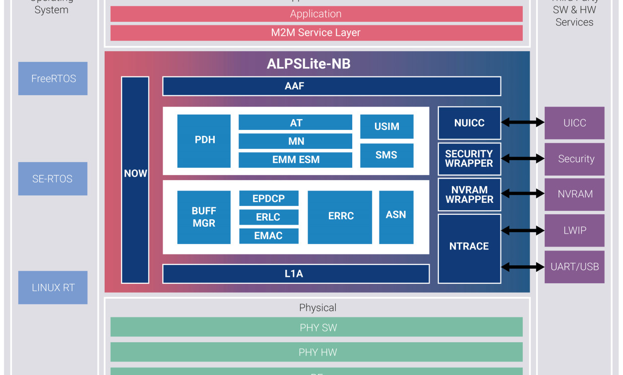
The internal architecture (Figure 1) and design need to account for optimal trade-offs between performance and memory, as well as the fact that single core solutions with integrated service layer (e.g. latest LwM2M from OMA), application, and layer 1 are now a reality.
[Figure 1 | Internal architecture of NextG-Com’s ALPSLite-NB]
Power optimization
Power saving needs to be at the center of the design efforts and architecture, as it is an important differentiating factor for the SoC.
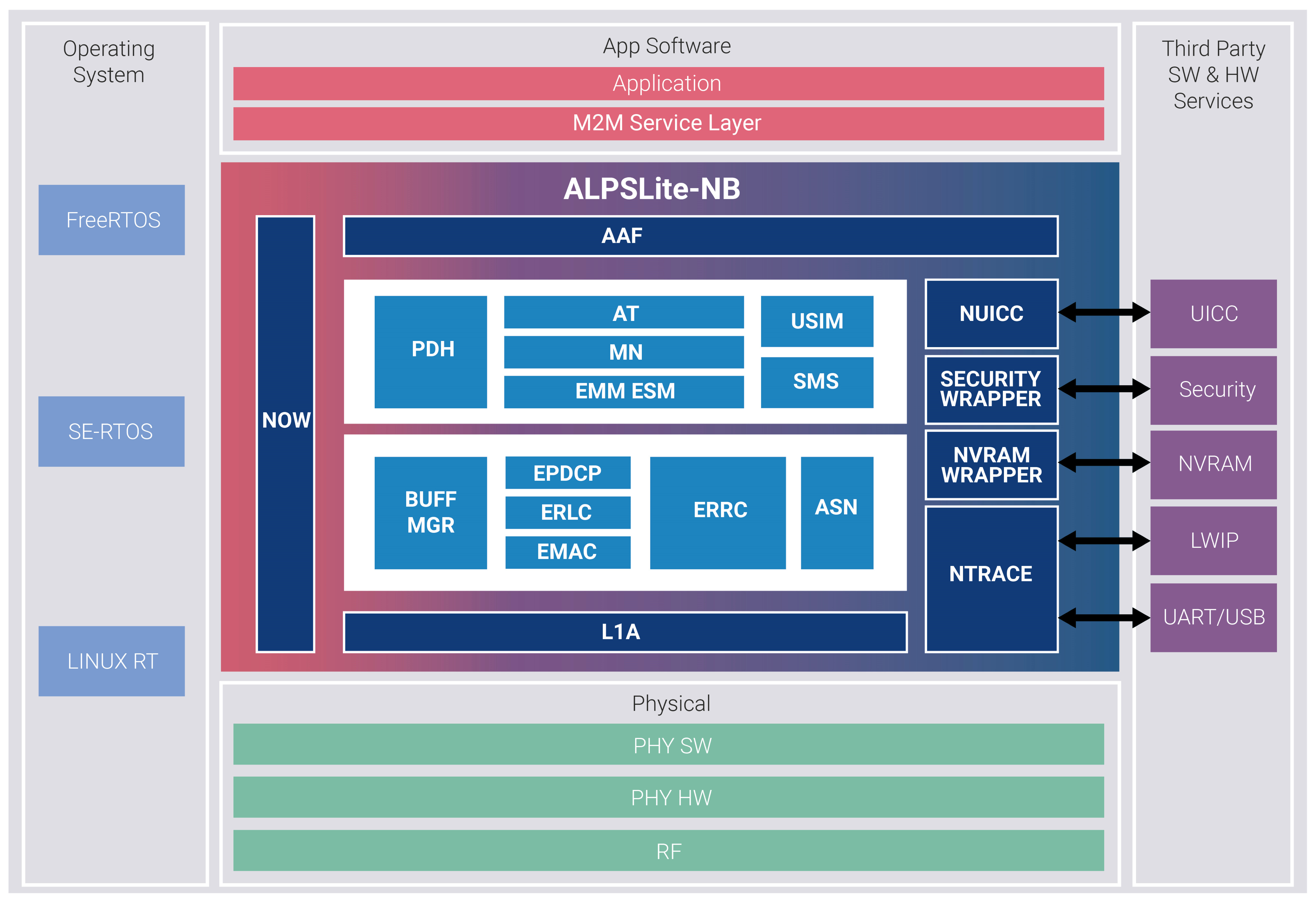
Techniques implemented in the standard, like power saving mode (PSM) and enhanced discontinuous reception (eDRX), allow the optimal power usage for application, which can, for instance, go to deep sleep for long period of time and/or require some level of latency on the receiving side. Even more importantly, the software in the SoC needs to take into consideration various application, network, and platform input parameters and make decisions to allow, for example, optimal sleep and wakeup cycles (Figure 2).
[Figure 2 | NextG-Com Single Core Integrated Power Module design]
SoC architecture optimizations
Consider an SoC designed around the CEVA-X1 processor. A number of built-in features have been specifically added to minimize cost and power to fit the ultra-low requirements of LPWA networks and use cases. For example, the cache memory sub-system should be carefully designed to find the optimal tradeoff between performance and area. On the program side, the protocol stack resides entirely in embed Flash, which has high access latency and requires the smallest program cache that will hide eFlash latencies without adding too much cache area. The L1 cache offers hardware prefetch to combine misses from the same cache line into a single request. The data memory sub-system uses a flat memory with embedded data RAM, but no data cache.

[Figure 3 | Program memory sub-system]
The low data rate of cellular IoT and the half duplex operation of NB-IoT Rx and Tx provide enough margin to run Rx and Tx in a time multiplexed fashion, and the loose round trip latency requirements allow protocol and baseband to run in a time share fashion on the same CPU/DSP processor. Dedicated instructions for NB-IoT allow for the increase of CPU MIPS required, and therefore reduce overall power consumption. Low data rate cellular standards are better served by specific instructions rather than by dedicated hardware accelerators since the data packets are small and the data rate is very low. The overhead of transferring small packets back and forth to off-core hardware accelerators becomes greater than the processing time itself. Dedicated instructions reside inside the core and use on-core registers and RAM.

[Figure 4 | NB-IoT SoC architecture]
The low duty cycle of processing and transferring data to the cloud and the half duplex nature of all software tasks allow for a complex multi-task use case such as an asset tracker with outdoor positioning through GPS and/or Beidou on the same SoC as the NB-IoT device, simply by adding code to the eFlash without requiring a high processor clock rate.
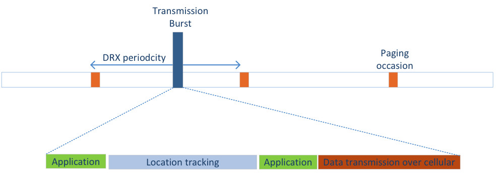
[Figure 5 | Asset tracker timing diagram]
All of the above software and hardware optimizations contribute greatly to area, power, and performance optimization with maximal gates reused. There is no dedicated hardware for a specific task, and the on-chip SRAM and cache are minimized.


