
A Resilient Error Correction Scheme for 3D TLC NAND
May 06, 2019
Story

Due to the complexity of 3D structures, several kinds of errors can occur. Especially in high-capacity systems, these issues require NAND flash controllers and advanced error correction algorithms.
In NAND process development, 2D NAND has reached its limits at about 10 nm. Because there are fewer electrons inside the floating gates of planar NAND technologies, 3D NAND structures are becoming mainstream in large-capacity storage systems.
3D NAND structures turn the planar floating gates 90 degrees, and stack many layers on top of each other to increase capacity. Most players in the 3D NAND market – including Samsung, Toshiba/WD, Micron, Hynix, and Intel – now mass produce 64-layer triple-level cell (TLC) NAND with die capacities of 256 Gb. 96-layer, 512 Gb options should be available at some point this year.
Overcoming Complexities of 3D NAND with ECC
Due to the complexity of 3D structures, several kinds of errors can occur. These include layer-to-layer read disturbance, write interference, and data retention problems. Especially in high-capacity systems, all of these issues require NAND flash controllers at the very least, and more specifically, advanced error correction algorithms.
Unfortunately, traditional Bose–Chaudhuri–Hocquenghem (BCH) error correction code (ECC) algorithms used in multi-level cell (MLC) NAND technology are not sufficient for 3D TLC NAND. More powerful low-density parity check (LPDC) ECC algorithms are required.
LPDC ECC uses both hardware and software mechanisms to correct bit errors. The hardware mechanism can correct more than 120 bit errors per 1 KB, while the software mechanism uses a more complex error correction methodology to resolve almost twice that many. But although they are more powerful, the software-based ECC operations take much longer to perform.
In addition to the hardware and software correction mechanisms, 3D NAND also requires a method of preventing mass data loss. This means that a RAID function must be implemented inside of NAND controllers that can resolve errors that can't be corrected by LPDC ECC algorithms, such as whole page errors or the corruption of several data pages. This RAID function of course requires some extra memory for parity and additional computational resources, but it's well worth it to ensure that the data on your SSD is secure.
Secure Data Sequence for 3D TLC NAND Devices
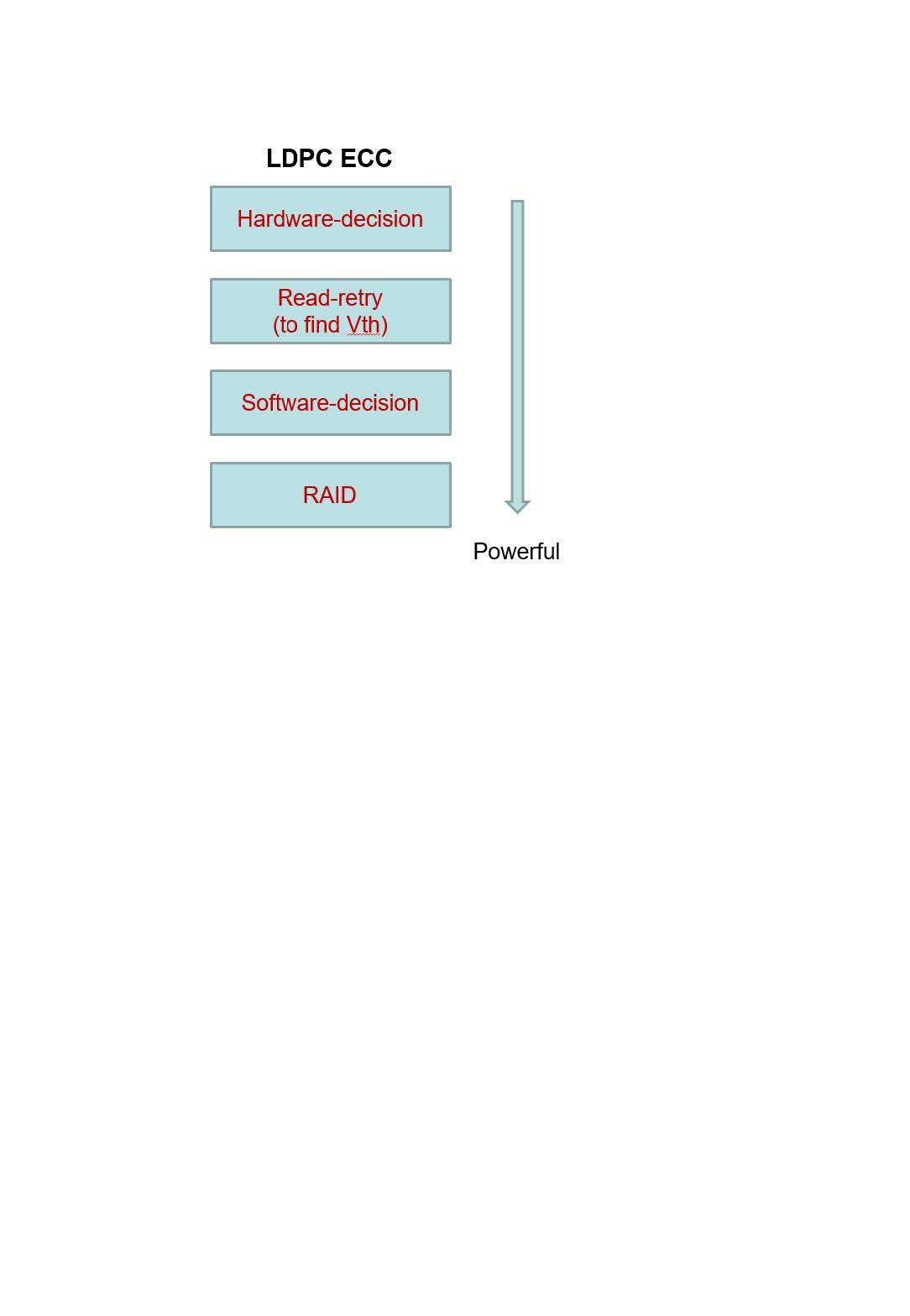
Figure 1 shows the LDPC ECC sequence for an SSD controller, including the aforementioned RAID function. In steps, the ECC sequence an SSD controller must implement is as follows:
- First use the hardware mechanism (hardware-decision)
- If step 1 fails try implementing different Vth (voltage levels of NAND states) to get the lowest bit error rate, also known as read shift or read retry
- Next, implement the software mechanism (software-decision) to correct the error
- If all else fails, use the internal RAID function
More Reliable 3D TLC NAND
3D TLC NAND represents and inflection point in storage media, providing a lower-cost-per bit and reduced footprint. For the market to expand into embedded industries, however, the technology will need to provide a sustainable, scalable suite of solutions for bit error correction.
By implementing the LPDC ECC sequence described above that terminates in a powerful RAID function on a NAND controller, UDInfo believes that SSD quality and data integrity can be guaranteed for the 3D TLC NAND-based devices of the future.


