
Designing High Reliability in Electronic Gaming Machines
January 05, 2021
Blog
Because the stakes can be high, gaming machines must be able to securely preserve all of this information in case of a power outage, power glitch, or machine failure.
Electronic systems that handle financial data require a high level of reliability. Casino gaming machines are no exception. These machines store and/or have access to sensitive personal and financial information, including player data and current credits. Players are also able to access comp funds and stored credits, and these financial transactions can represent thousands of dollars or more. Gaming machines also need to store a wide range of critical operational information such as user key presses, payout ratios, and winning statistics.
Because the stakes can be high, gaming machines must be able to securely preserve all of this information in case of a power outage, power glitch, or machine failure. Typically, when an embedded system fails, it defaults back to a safe mode that allows mission-critical capabilities to continue uninterrupted. For example, a plane has to stay operational to prevent it from crashing.
The opposite is true of a casino gaming machine. When there is a failure, standard operating procedure is to ensure that the machine is protected and not to clear the error condition. At this point, the gaming commission becomes involved and commonly recommends the machine undergo forensic analysis to determine the cause of failure and to create a chain of evidence log for potential litigation purposes. For example, if a player hit a large jackpot just before the failure, this evidence log will be crucial for establishing whether the jackpot is accepted or disqualified.

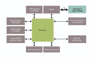
(Figure 1: Block diagram of a gaming machine.)
In addition to storing player and operational data, the system will also need to store an image of the gaming algorithms the FPGAs and/or MPUs are using (see Figure 1). Furthermore, the operational execution state and system stack need to be logged as well. The data in these logs is important in establishing the integrity of the gaming machine and of casino operators in cases where they are accused of malpractice.
All these requirements together create a challenging problem for engineers. The extensive amount of data that must be stored securely requires high density memory. In addition, the memory subsystem must be extremely fast to prevent data loss during a power outage.
Non-Volatile Memory
First and foremost, non-volatile memory is essential. Traditionally, gaming machines have used battery-backed SRAM to preserve memory effectively. However, this approach does not provide sufficient reliability. Battery-backed SRAM requires multiple components and consumes more PCB area than a native non-volatile memory chip alone. Batteries are typically mounted after the reflow process to avoid exposing them to heat, which increases manufacturing cost. Batteries also require on-schedule maintenance and replacement. Such maintenance increases operating expenses. If the gaming machine employs tactical feedback like buzzing or shaking, such vibration can lead to failure of the mechanical joints holding batteries in place. Finally, batteries that do not comply with RoHS requirements create unwanted disposal challenges for casino operators.
For these reasons, manufacturers prefer to use battery-less non-volatile memory solution to store logged information. Table 1 shows several types of non-volatile memories. The limited endurance of EEPROM quickly eliminates it as a viable choice for logging in gaming machines that must operate continuously for multiple decades.

(Table 1: A comparison of different non-volatile memory types.)
Flash-based approaches, even though with limited endurance count like EEPROMs, increase the lifetime of memory using a technique called wear leveling. Software on the MCU employs a complex algorithm to identify when a block of memory is worn and begins to experience errors beyond a set threshold. The algorithm then searches for another block that is not worn and moves the data to that block. Wear leveling algorithms tend to try to spread wear evenly throughout the Flash device. This makes wear leveling a fairly complex process that, while increasing reliability, ultimately adds latency to write operations.
Flash writes take place in pages, which also has a significant impact on write performance. Typically, data to be logged will be captured and collected in a buffer until a full block is available to write. Next, the block in memory to write to must be identified by the wear leveling algorithm, which can involve software-based look-up within large data tables. With Flash, the block must first be erased before it can be written to. Finally, the data buffer is written to memory.
Real-Time Capture
When the power fails, the system has little to no time to react. Thus, for gaming machine data to be stored with high reliability, the data must be captured and stored continuously. The worst case scenario is when a power failure occurs during a gaming event since this is when there is the most real-time data to collect and potentially the least amount of time in which to capture it.
If a failure occurs any time during the Flash write process, data in the buffer will be lost. The longer the write process, the greater the risk of losing data crucial for understanding why the machine failed and establishing the integrity of the casino operator.
To minimize write time and increase overall reliability, manufacturers are turning to highly reliable NVRAM solution such as Ferroelectric Random Access Memory (F-RAM). As a non-volatile memory technology, F-RAM offers many advantages for data logging applications over battery-backed SRAM, EEPROM, and Flash. F-RAM has an extremely high endurance – 10^14 cycles – which is effectively unlimited for a logging application. With such a high endurance, no wear leveling is required, simplifying the write process.
Furthermore, F-RAM is a random access technology, and there is no need for a buffer and that writes can be performed directly into nonvolatile memory cells without a separate erase cycle first. This means that as data is collected, it is can be immediately stored in non-volatile memory. Random access also eliminates the latency associated with memory paging. Thus, logged data can be written “instantly” as compared to the relatively long window required by Flash using a buffer (see Figure 2).

(Figure 2: The latency of capturing data in a buffer and only writing it to Flash when the buffer is full places crucial data at risk. If a power failure occurs during this time, important forensic data will be lost. b) Because of its random access nature, captured data can be immediately written to F-RAM. This eliminates the “soak time” of EEPROM, minimizing time at risk and data loss.)
To provide higher reliability, F-RAM memory includes on-chip error code correction (ECC) to detect and correct bit errors. In addition, F-RAM reads are destructive. Thus, any bit flip in the F-RAM array is detected and corrected with ECC when the data is read, and the corrected data is written back into the array. This ensures even greater reliability as well as increases the longevity of the F-RAM as a whole.
F-RAM connects to a standard memory controller over a serial interface like SPI. The use of a serial interface compared to the parallel interfaces used by battery-backed SRAM free up processor pins, allow developers to select a more compact MCU package, shrink bus traces, and reduce board size.
F-RAM, such as Excelon F-RAM from Infineon Technologies, is available in industrial and automotive grades to assure high reliability under extreme operating conditions. For example, industrial F-RAM can store data up to 10 years at a maximum temperature of 85 °C, with an increase to 151 years at 60 °C. These memories are also available with a high-performance 108 MHZ Quad SPI interface that enables them to provide performance on par with parallel battery-backed SRAMs.
Data and Code
Because of its contiguous, random access nature, a single F-RAM device can be used for both data logging and code memory. Effectively, a single memory can replace ROM and RAM devices as F-RAM provides the functionality of both SRAM and Flash. Combining data and code in a single memory device can simplify system design and reduce overall cost. In addition, storing algorithmic code in F-RAM automatically preserves the code image the system was using at time of failure, which can be extremely useful during failure forensics.
To support the reliable memory requirements of applications like gaming machines, F-RAM is available in high densities, currently up to 8 Mbits with 16 Mbit devices sampling in early 2021.
Today’s casino operators need highly reliable gaming machines to protect their interests in cases where machines fail or lose power at an inopportune time. Current battery-backed SRAM systems lack physical robustness, increase system cost, and incur ongoing maintenance expenses. Flash-based systems can preserve data during power outages but can also lose their buffer, which has the most crucial data for understanding why and how a gaming system failed. By working with F-RAM, developers can create data logging systems that offer the highest reliability by writing data as it is captured, ensuring that casino operators will have the data they need to establish a chain of evidence and successfully pass forensic analysis.
About the Authors
Shivendra Singh is an Applications Er. Sr. Principal at Cypress Semiconductor. He has more than 13 years of experience with various volatile and nonvolatile memory products, technologies, and system solutions. His current responsibilities include, but are not limited to, creating new product definitions and specifications, product failure analysis, developing validation platforms, demos and development kits, design models, and customer trainings. Shivendra has published several technical articles on various topics including RAID, RTC, Wearable, and Automotive EDR in leading technical journals as well as has authored many technical documents that include application notes on design, whitepapers, knowledge base articles, available on www.cypress.com. He can be reached at [email protected].
Karthik Rangarajan is a senior staff product marketing engineer at Infineon Technologies. He is involved in defining market entry strategies for semiconductor ICs across a broad spectrum of end markets. He has worked for Oracle and Deloitte and has a management degree from IIM, Bangalore and an engineering degree from BITS, Pilani. He can be reached at [email protected].


