
Applied Materials' Endura High-Volume Manufacturing Platforms Deliver Precision for Next-Gen MRAM, ReRAM, PCRAM Memories
July 09, 2019
News
The Endura platforms feature on-board metrology that enables new films, structures, 3D architectures, and the precision needed for advanced chip memories with improved power, performance, and cost.
Applied Materials has released its Endura platforms, new high-volume manufacturing solutions for MRAM, ReRAM, and PCRAM memory technologies. The advanced memory technologies target IoT and cloud computing deployments, but are based on new materials that require atomic-level precision. The Endura platforms feature on-board metrology that enables new films, structures, and 3D architectures, as well as the manufacturing precision needed to produce advanced chip memories with improved power, performance, and cost.
Magnetic Random Access Memory (MRAM) is an inherently fast, non-volatile memory technology that incorporates delicate magnetic materials often found in HDDs, and at least 30 different layers of material in total. Some of these layers – which can be 500,000-times thinner than a human hair – allow MRAM devices to retain data even when power is lost or removed, and make the technology a leading candidate to replace SRAM in level 3 cache memory. MRAM can be connected into the backend interconnect of chip designs, which promotes smaller die sizes.
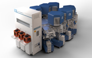
Applied Materials’ Endura Clover MRAM PVD platform is a 300 mm MRAM manufacturing system that consists of nine wafer processing chambers. These high-vacuum chambers are capable of depositing five different materials per chamber, while on-board metrology measures the thickness of MRAM layers with sub-angstrom sensitivity to reduce the risk of process variations that can adversely affect device performance.

Resistive RAM (ReRAM) and Phase-Change RAM (PCRAM) are other fast, low-power, non-volatile, high-density memories that target storage-class memory in servers. ReRAM is built on materials that selectively form filaments that represent data within storage cells. PCRAM, on the other hand, uses the same phase-change material found in DVDs, where bits are programmed by changing the material state from amorphous to crystalline.
Both ReRAM and PCRAM are arranged in 3D structures and support intermediate layers of programming and resistivity so that multiple bits can be stored within a memory cell. These features allow more layers and bits-per-cell to be supported in successive product generations, thereby significantly reducing costs compared to DRAM.
The technologies offer substantially faster performance than NAND or HDD solutions, while ReRAM projects to be a leading candidate for in-memory computing architectures that will be required for AI computing.
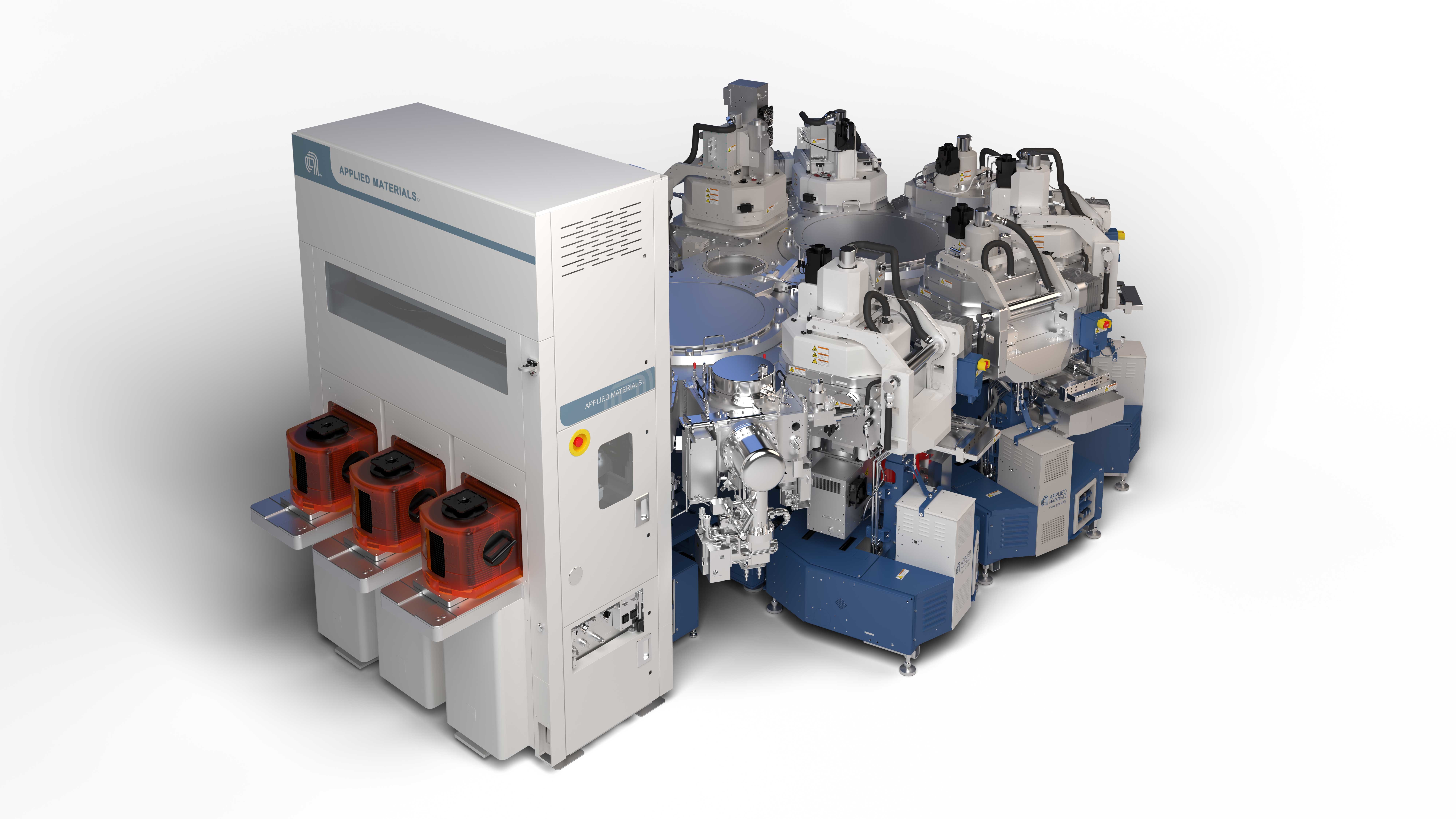
The Applied Materials Endura Impulse PVD platform incorporates nine process chambers as well as an on-board metrology system, which deliver the precise deposition and control of multi-component materials used in ReRAM and PCRAM devices.
For more information on advances in semiconductor manufacturing, visit www.appliedmaterials.com.


