
All-in-One Power Solution for Automotive Infotainment?Single IC Produces Five Rails Directly from Battery
April 02, 2019
Story

The complex mix of electronic components contained in automobile infotainment systems mirrors consumer electronics: high performance microcontrollers, memory, interface, and driver ICs.
Our connected and media driven lifestyles are a result of, or a reason for, technology’s push into every aspect of our lives, including today’s highly integrated automotive infotainment systems. The complex mix of electronic components contained in automobile infotainment systems mirrors consumer electronics: high performance microcontrollers, memory, interface, and driver ICs.
The power supply picture is just as complex, as each component may require a variety of low voltage rails with wide ranging power requirements. Complexity is not limited to the infotainment systems. Automotive performance, fuel efficiency, and driver convenience features require increasingly advanced electronic systems. The power system also stands between sensitive electronics and the unwelcoming conditions of the automotive setting—namely the wide-ranging voltage and predictably transient battery environment serving as input. A well-designed power system must both power and protect electronics, even as manufacturers make the automotive environment less inviting to electronics with features such as start-stop technology.
Start-stop technology magnifies the extreme conditions that electronics must face, specifically through repeated engine cranking. A start-stop enabled car restarts the engine repeatedly, but critical systems must remain operational even as the battery supply goes through a cold crank each time—while not catastrophic, a driver suddenly singing acapella as the car’s music goes silent may not add to the car’s positive reviews.
At the other end of the spectrum, ultralow quiescent current is a critical requirement of automobile power systems. An automobile may need to sit unused for a month or more as critical always-on electronic systems quietly run, without draining the battery.
The ADI Power by Linear LTC3372 all-in-one high voltage controller is capable of maintaining regulation through the extreme voltage changes presented by automotive battery environments. It can keep always-on components running without draining the battery because of its ultralow quiescent current. The LTC3372 features four configurable monolithic regulators and can provide up to five output channels for infotainment or other electronic systems.
Automotive Multichannel Power
The LTC3372 significantly reduces the number of components required to produce multiple rails. It combines proven high voltage automotive controller technology with four configurable monolithic bucks to create a space- and cost-efficient automotive multichannel power solution.
The high voltage buck controller input operates through input surges up to 60 V, such as those seen during a load dump, and can also regulate through input dips as low as 4.5 V in a standard buck configuration, and down to 3 V in a SEPIC configuration. This operating input range enables uninterrupted power to sensitive electronics in the face of significant transients. The LTC3372’s four low voltage bucks are configured independently by combining power stages from a selection of eight 1 A power stages. Stages are combined to meet the power requirements of each regulator, with eight possible unique 4-output channel configurations, all directly from an automotive battery source.
One benefit of a single IC multichannel power solution is shared internal voltage references and bias supplies. This bias sharing enables lower per channel IQ specifications for multichannel power than would be available with independent ICs. For a single-channel, always-on supply, the VIN referenced bias IQ is 23 µA typical and 46 µA maximum at 150°C. With all five channels regulating in Burst Mode® operation, the typical bias current is only 60 µA total, or 12 µA per channel. The LTC3372 enables new always-on applications when its total bias IQ for five channels is comparable to a single channel using older technology.
Single-Chip Controller and Regulators
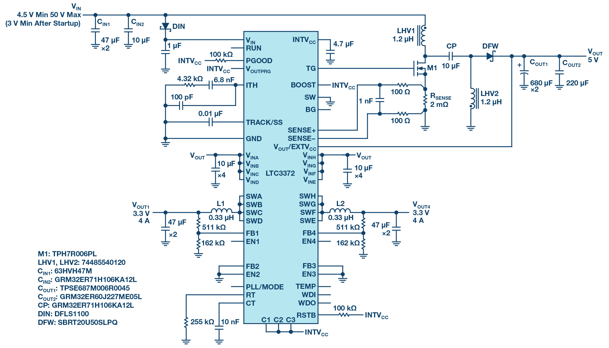
The LTC3372 is a front-end 60 V high voltage (HV) buck controller plus four low voltage (LV) 5 V monolithic buck regulators with low IQ Burst Mode operation. By integrating a controller and monolithic regulators, LTC3372 can provide up to five separate rails from high input voltage in compact size at low cost. The output voltage of the HV controller can be selected between 3.3 V and 5 V depending on the level of VOUTPRG pin; the output voltages of the LV regulators can be individually programmed with external resistors through FB1 to FB4 pins.
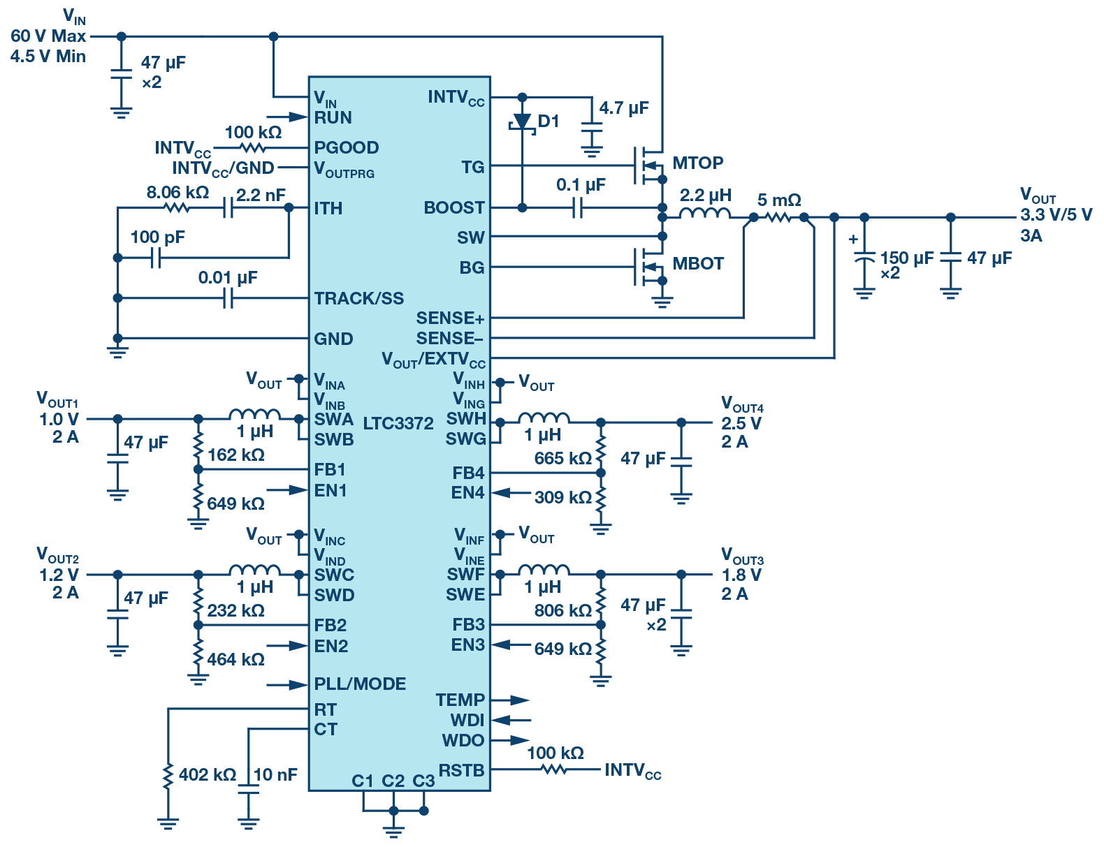
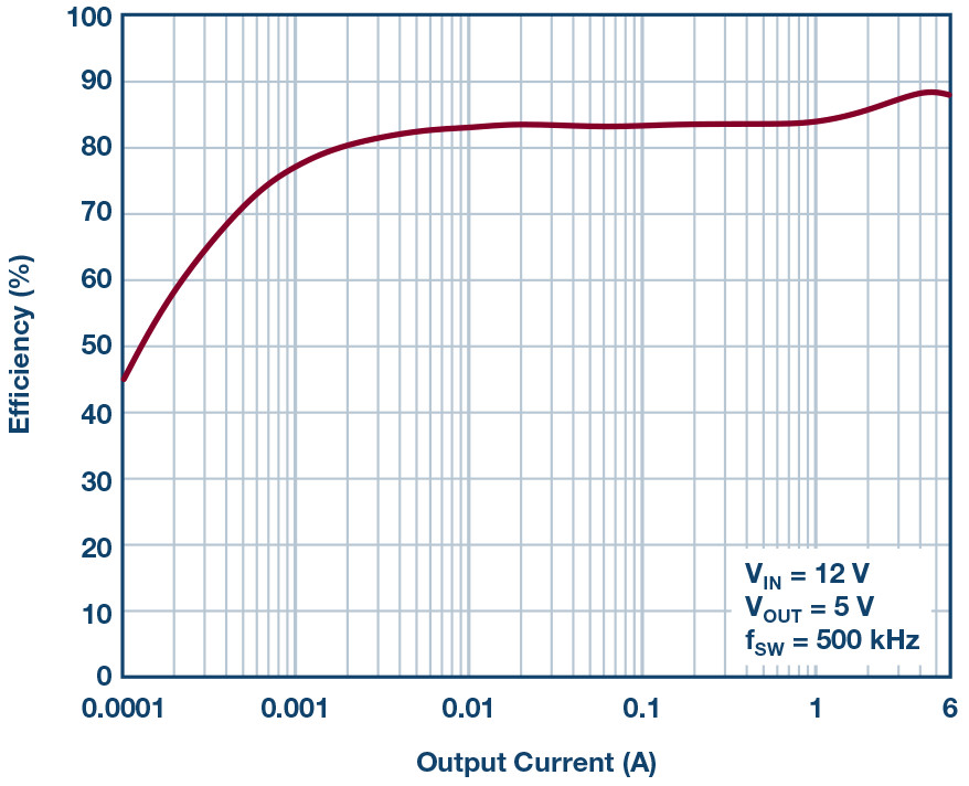
Figure 1 and Figure 2 show a typical application and the corresponding efficiency of the HV controller. While the HV controller is typically used for feeding the LV regulators, each regulator operates independently via per channel to enable and input pins. Additional flexibility is provided by the eight power stages. The eight switches can be distributed among the LV regulators, with the combination digitally configured through the C bit (C1, C2, C3) to meet rail-specific maximum current limits. Table 1 shows C bit settings and the resulting maximum current limit configurations per regulator number. Figure 3 shows how efficiency varies with the number of switches combined in parallel.

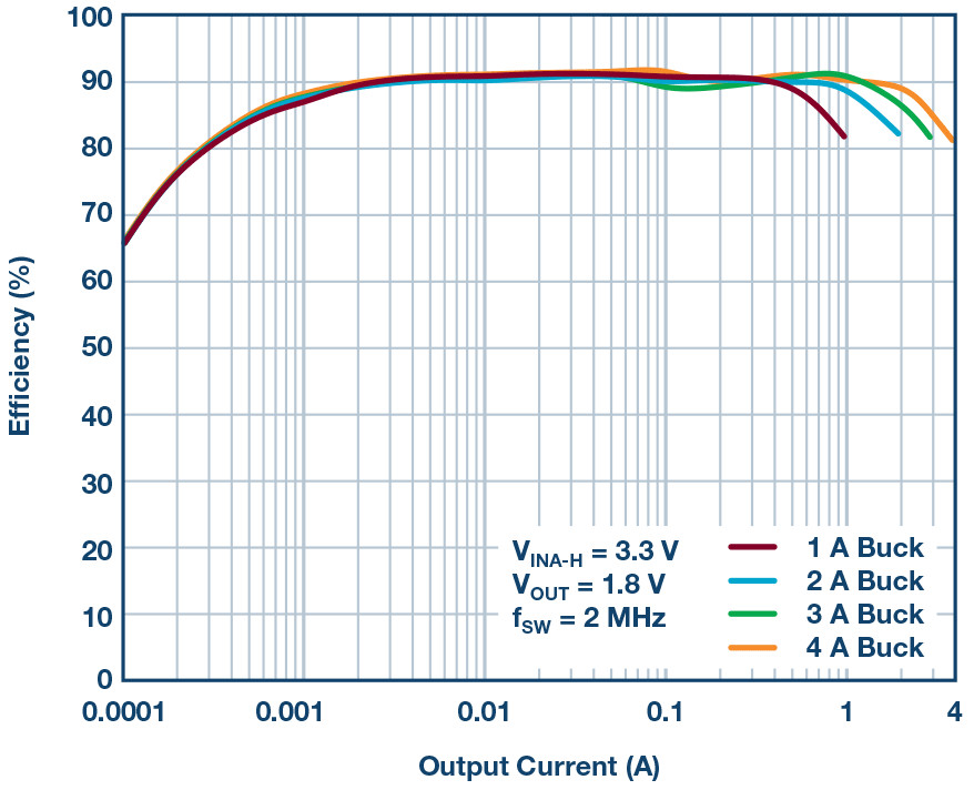

Table 1. LV Regulator Configurations Are Set via C1, C2, and C3 Codes; In Any Configuration of Fewer Than Four LV Regulators, the Unused Regulators Enable Pins and Feedback Pins Are Connected to Ground
Power Loss Optimization
The LTC3372 also provides an on-chip temperature sensor and watchdog timer features. The temperature sensor allows users to closely monitor die temperature whenever a LV regulator is enabled. The watchdog timer issues a reset signal if the microprocessor fails to clear the timer when malfunction occurs.
Often, dc-to-dc converters are judged on their efficiency and are therefore designed to maximize that parameter, but optimizing dc-to-dc converters in terms of power loss (instead of just efficiency) usually pays higher performance dividends in high power applications. For a multistage converter system, such as can be created with the LTC3372, efficiency measurements can be misleading when some part of the efficiency is the composite of HV controller and LV regulators.
Keep in mind that power loss optimization does not mean simply minimizing total power loss, but also balancing the distribution of the losses across devices. A good approach is to begin with the LV regulators, as the total power loss across all LV regulators accounts for most of the loss in the LTC3372 system. By considering all applicable LV regulator configurations, a designer can compare a significant range of power loss options. Table 2 lists all applicable configurations and the associated power loss in a 1.2 V, 1.8 V, 2.5 V application at 3 A, 3 A, 0.5 A maximum load, respectively. The difference between the best and the worst configurations is 0.432 W. In normal cases, recursively allocating the largest possible switch to the highest power channel yields the best result.
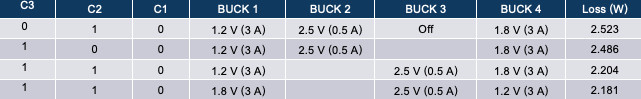
Table 2. Total Burst Mode Operation Power Loss in LV Regulators of 1.2 V (3 A), 1.8 V (3 A), 2.5 V (0.5 A) in Various Configurations; VINA–H are 3.3 V and Switching Frequency is 2 MHz; The Best Configuration Yields 0.432 W Less Power Loss Compared to the Worst Case
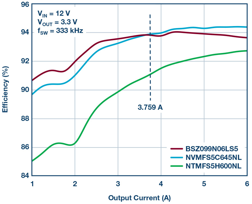
More generic efficiency optimization procedures can be applied to the HV controller. The slight difference is that all/part of the HV controller’s loading becomes the input referred current of LV regulators. When LV regulators are the only loads, the HV controller sees a moderate load, even if each LV regulator is fully loaded. Instead of selecting the low RDS FETs or pursuing the highest peak efficiency, designers should focus on the operating current range of interest. The efficiency vs. output current curves of three FETs with distinct RDS are shown in Figure 4. For the LV regulators in Table 2, using the highest RDS but lowest QG FET yields the highest efficiency in the range below maximum load (3.759 A in the optimum configuration).
SEPIC Controller
In automotive applications, cold crank remains a challenge to dc-to-dc converters. Buck converters are forced to operate in dropout if the regulated output voltage is higher than the input in cold cranking situations. Two alternative front-end topologies, boost and SEPIC, can be realized using available resources provided in the LTC3372’s HV controller to avoid dropout operation.
Even though the boost is slightly simpler, it passes any high voltage input surge to the following buck stage. This precludes the use of high efficiency low voltage buck regulators as the second step-down stage. In Figure 5, we configure the LTC3372 HV controller in a nonsynchronous SEPIC topology. The SEPIC converter generates a 5 V intermediate rail to power two 3.3 V/4 A LV regulators and to sustain the continuous operation of HV controller.
When two 4 A LV regulators are fully loaded, more than 5 A of current is drawn from the SEPIC output. The peak current through the sense resistor can easily exceed 10 A as the switch current is the summation of both inductor windings. Considering that the sense resistor is within the hot loop, some effort is required to produce a clean waveform at the current comparator inputs. One solution is to incorporate a differential filtering scheme as shown in the SEPIC schematic, and use a low inductance resistor fabricated in a reversed package.
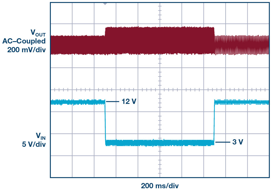
Figure 6 shows SEPIC efficiency in Burst Mode operation and Figure 7 shows the SEPIC output voltage when a 12 V-to-3 V transient is applied to the input. Designers should not overlook the heat generated in the catch diode during PCB design. Thermal limits can be met by reserving extra space for a moderately oversized diode and using thicker copper. Another diode and a filtering capacitor are connected to the VIN pin to avoid reversed current and sudden voltage spike due to input transients.
Conclusion
The LTC3372 provides a single chip solution for high voltage multichannel buck converters. Its low IQ operation and low cost per channel are a good fit for always-on systems in automotive applications.
About the Authors
Jin-Jyh Su joined Linear Technology (now part of Analog Devices) as an analog IC design engineer after graduating from the Georgia Institute of Technology. He was with the Linear Analog Device Power Group in Milpitas, California and Dallas, Texas for three years. Su specializes in high performance dc-to-dc converter design. His design experience includes monolithic and controller products operating at high voltage (100 V), high speed (3 MHz), and low IQ for automotive applications. Su recently joined the Battery Management System (BMS) Group in Dallas, Texas where he is working on multicell battery stack monitors. He can be reached at [email protected].
Terry Groom is a power design section leader and has been with Analog Devices for almost 13 years. He is a graduate of Texas A&M and Georgia Institute of Technology. Groom’s design group, located in Dallas, Texas, specializes in high performance dc-to-dc power controllers. He and his team have developed products with voltage inputs from 5 V to 150 V in multiple switch mode topologies with switching frequencies of up to 3 MHz. Groom has more than 30 years of direct design experience in a variety of analog disciplines. He is proud to be a valued member of the Analog Devices’ Power by Linear development team. He can be reached at [email protected].


