
Peak-to-Peak Frequency Monitoring
October 06, 2020
Story
The peak-to-peak method is used with real-world analog signals, often originating from analog sensors.
Frequency monitoring circuits are addressed in several varieties. A ''zero-crossing detector'' is considered one of the most common methods due to its simplicity of design for periodic and regular signals. However, if the signal is aperiodic or irregular (contains a non-instantaneous zero period between pulses) zero-crossing cannot be used. In such cases a peak to peak frequency monitor is a desired alternative.
The peak-to-peak method is used with real-world analog signals, often originating from analog sensors. The design described in the this article uses the SLG46620V GreenPAK™ to calculate the low-end frequency for signals ranging from 0.5 Hz to 200 Hz and whose waveform width is between 100 - 1000 ms. With a fundamental understanding of this application the peak-to-peak measurement of other analog widths and periods can be designed.
The circuit comprises all parts of the peak-to-peak design. Thus, the IC is responsible for receiving an analog signal sample and storing identified peaks in an internal buffer. It is also responsible for comparing the measured time period between two peaks with internal thresholds to give a signal when these thresholds are exceeded.
The design is made up of one analog signal input and 4 outputs:
- PD: To give a pulse when the peak is detected.
- High PPM: Gives HIGH if the signal frequency exceeds the upper threshold.
- Low PPM: Gives HIGH if the signal frequency exceeds the lower threshold.
- Normal: Gives HIGH if the frequency is within the two thresholds.
The IC’s Analog-to-Digital Converter (ADC) macrocell provides a fit for peak signal detection. The chosen circuit is low-power and cost-effective. It is a small device as required in this application. The IC can substitute for a system of discrete ICs and passive devices.
The general circuit is explained with the expectation that it will be augmented to fit a particular, real-world application. The results of the design utilize the GreenPAK Designer software signal generator to test varied signals and display the corresponding output. Signals are generated at higher and lower frequency than the values stored in the IC and the corresponding output for each case is displayed to confirm correct operation to the reader.
The complete design file of this application can be found here.
Design Overview
The detection process samples an analog signal using the ADC block, then stores it in an internal buffer. A new sample of the analog signal is then received and compared to the stored sample.
If the new sample's value is greater than the currently stored value, the analog voltage is increasing. The new sample is stored in the buffer and the next sample of the signal is received and compared. But, if the received sample equals the stored sample in the buffer, the signal is constant. At this point either it reached a short constant value but not reached the peak, or it has reached the peak, so the peak state is only considered when the signal begins to fall.
If the next sample is smaller than the previous one stored in ADC buffer, then a peak state is recorded. The process is repeated at another cycle to find the next peak.
To calculate frequency, we calculate time between two consecutive peaks and this time is compared to certain thresholds that are pre-stored in the internal registers of the IC. If this time is greater than the higher threshold, the frequency is less than the allowed limit. If this time is less than the lower threshold, the frequency is greater than the allowed limit.
Since the design is suitable for relatively low-frequency signals, they are usually calculated in pulses per minute, abbreviated in this context to PPM. Thresholds are labeled as High PPM and Low PPM.
To ensure that all recorded peaks are desired, each peak will be compared to a pre-stored voltage threshold so that a peak is only considered if its amplitude is greater than the chosen threshold, and short-amplitude signals are ignored. Figure 1 shows the working process.
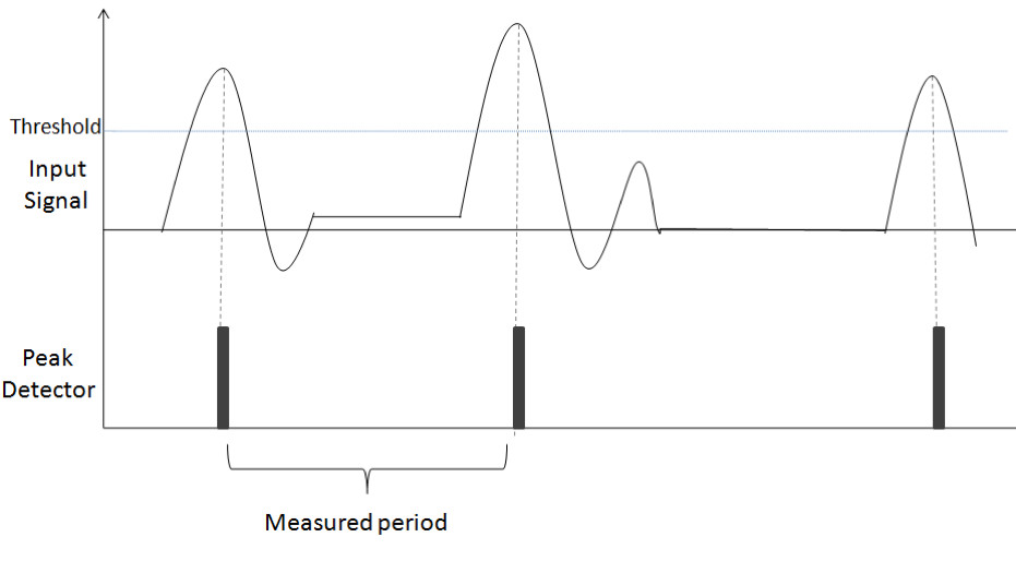
(Figure 1: System Working Process)
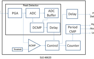
GreenPAK Design
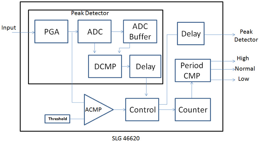
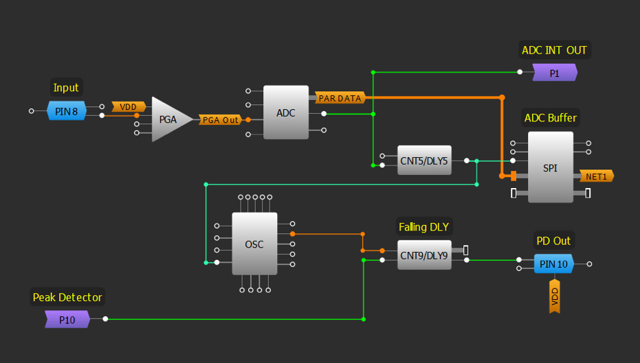
The design consists of two parts: a peak detector circuit and a frequency monitor circuit, which contains a timer and threshold comparator. Figure 2 shows the block diagram of the design.
(Figure 2: Circuit Block Diagram)
Peak Detector
The IC receives the external signal through Pin 8, which is configured to operate as an analog input/output. The signal then passes through a programmable gain amplifier, or PGA, which sets the gain. The operation mode of ADC is single-ended and a x1 gain is set. Then, the signal enters the ADC block.
In this design the input signal is low frequency, so the sample rate is reduced by dividing the clock cycles by 16. The sample rate becomes equivalent to 97,6563 sps to reduce error values and spikes.
Sample rate = PWM & ADC clock / 256 = 25k / 16 / 256
To indicate a peak, a signal must be given to indicate whether the analog input is rising or falling. To do this, two consecutive values from the ADC output must be compared. The SLG46620V SPI block is configured to run as an ADC buffer.
According to ADC properties within datasheet, PAR data is ready to be used several clock cycles before the ADC INT output is activated. Taking advantage of this property, the ADC INT output is connected to the SCLK input of the SPI block via DLY5, which is configured to operate as a rising edge delay. Therefore, the comparison is made between the new ADC value and the old one with the rising edge of the ADC INT output signal. After a delay, the DLY5 output triggers SPI to store the new value in the buffer. The work timing diagram is clarified in Figure 3.
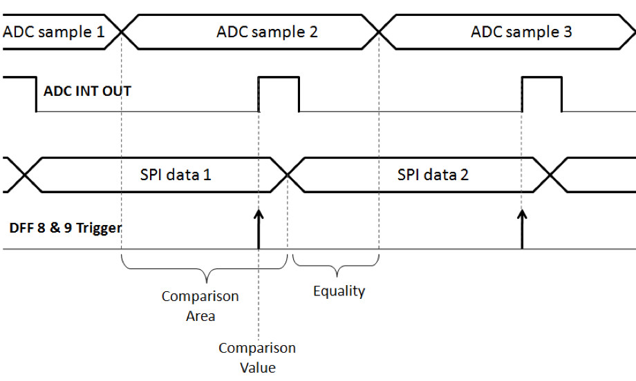
(Figure 3. ADC, SPI, and DFFs Timing Diagram)
(Figure 4. GreenPAK Design-Matrix 0)
The ADC value is compared to the buffered value via DCMP0, where the IN+ input takes its value from ADC [7:0] and the IN- input takes its value from SPI [7:0]. The EQ and OUT+ outputs are connected to DFF8 and DFF9 respectively.
If the ADC value is greater than the SPI value, then OUT+ = 1, and EQ = 0.
If the ADC value is less than the SPI value, then OUT+ = 0, and EQ = 0.
If the ADC value equals the SPI value, then OUT+ = 0, and EQ = 1.
The EQ and OUT+ outputs are held with the rising edge of the ADC INT output signal. To ensure that no equality state is recorded with each comparison, the SPI will trigger via DLY5 output. Thus, the comparison is only between two consecutive values as shown in Figure 3.
By monitoring the state of the EQ and OUT+ outputs during system operation, intermittent pulses are introduced that would cause glitches if left unaccounted. To prevent this and maintain a stable signal CNT3, CNT7, and CNT8 operate as delays to debounce the system. The effect of spikes on the output state can thus be prevented.
3-bit LUT8 operates as an SR latch, where the signal from the OUT+ output represents Set, indicating the signal is rising. Reset comes from 3-bit LUT9 which means the signal is falling.
3L9 is configured to give a High signal if the OUT+ = 0, EQ = 0 and the ACMP1 output is high.
The priority has been given to the rising state, as the aim of the system is to detect the highest value of the amplitude.
Once the signal starts to fall after a rising state, the 3L8 output will be changed from high to low and the falling edge is detected through P DLY1. The P DLY1 output indicates the detection of the peak (PD). The PD signal passes to Pin10 with an increase in pulse width through DLY9 to fit the sensitivity of any external device. It is also used to reset the counter.
ACMP1 is used to compare PGA output with a fixed threshold, chosen to be 200 mv in this design. Therefore, the peak will be ignored if its amplitude is less than the marginal value.
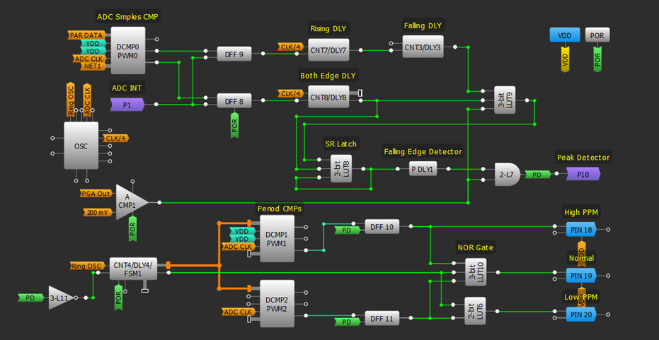
(Figure 5. GreenPAK Design-Matrix 1)
Peak to Peak Frequency Monitor Design
Having constructed the peak detector design, we will use the PD signal coming out of the said design to build a frequency monitor.
FSM1 serves as a counter to calculate the time between the two peaks. Since the expected signal is low frequency, the clock source for FMS1 has been selected as LF OSC, divided by 16. Therefore, measuring time can be between 19 ms and 2.35 s with a ~10 ms step. By using the low frequency oscillator active current consumption is minimized.
DCMP1 and DCMP2 compare the FSM1 value with the upper and lower frequency thresholds. DCMP1 compares the FSM1 value with the (1:1) register value, set as 500 ms in this design and represents the lower threshold. DCMP2 compares the FSM1 value to the register2 value, set as 897 ms in this design.
The compared value is stored in DFF10 and DFF11 along with the rising edge of the PD signal. Q output polarity has been configured to DFF11 to be inverted.
FSM1 data < Register0 value ---> DCMP1 OUT+ = HIGH ---> DFF10 out = HIGH ---> High PPM
FSM1 data > Register2 value ---> DCMP2 OUT+ = HIGH ---> DFF11 out = HIGH ---> Low PPM
Register0 < FSM1 data < Register2 ---> 3L10 out = HIGH ---> Normal
FSM1 resets with the falling edge of the PD signal through the 3L11 inverter. If the period exceeds the FSM1 work range of 2.35 s, FSM1 output provides a high signal to 3L10 and 2L6 to turn off all outputs. This case indicates the measured period is greater than intended. This function can be used to indicate that there are no pulses in the input or at a dangerously low period for the particular application. The clock source for the FSM can be changed to suit the application intended to be implemented.
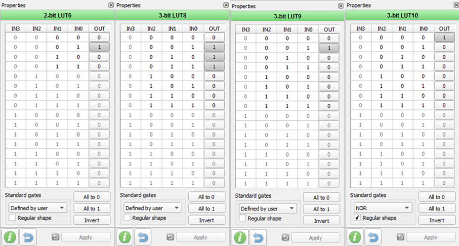
(Figure 6. LUTs Properties)
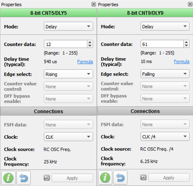
(Figure 7. CNT5 & CNT9 Properties)
Results
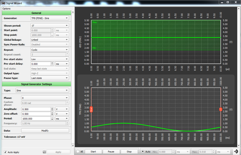
The signal wizard included in the GreenPAK Designer program has been used to examine the design and ensure it works as expected.
Signal Wizard is very convenient for design inspection, where signals of different shapes can be generated without the need to use an external signal generator. The signal frequency and amplitude can be easily controlled. A custom signal can also be generated.
Several signals were generated. The PD signal is displayed as shown in the figures below.
(Figure 8. CNT5 & CNT9 Properties)
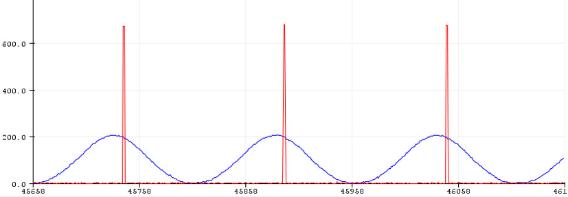
(Figure 9. Blue Signal Is Input, Red Signal Is PD Out Signal)
Generating a custom signal with a short undesirable peak.
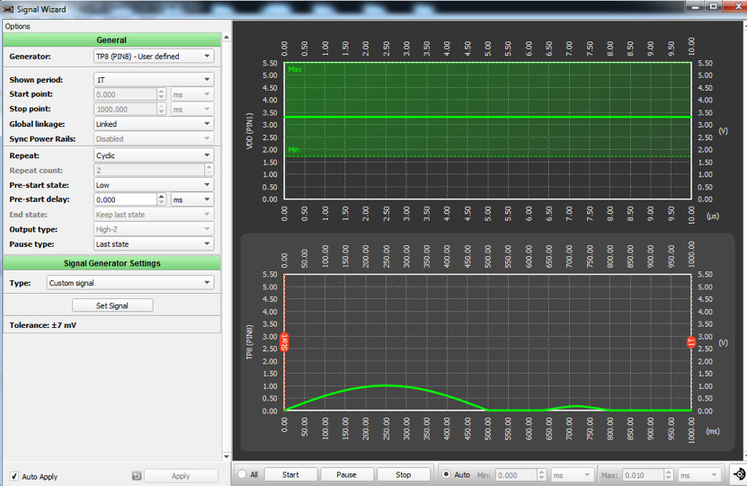
(Figure 10. Generating a Custom Signal)
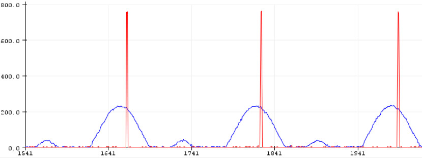
(Figure 11. Blue Signal Is Input, Red Signal Is PD Out Signal)
Different periods have been applied to the input. Corresponding output states are shown in Table 1.
Table 1: Output States for Different Periods
|
Peak to Peak Period on Input |
Pin18 Output (High PPM) |
Pin19 Output (Normal) |
Pin20 Output (Low PPM) |
Peak to Peak Period on Input |
|---|---|---|---|---|
|
400 ms |
High |
Low |
Low |
400 ms |
|
1000 ms |
Low |
Low |
High |
1000 ms |
|
800 ms |
Low |
High |
Low |
800 ms |
|
No signal |
Low |
Low |
Low |
No signal |
This article outlined how to build a peak detection circuit, which includes a frequency monitor circuit based on the peak-to-peak time calculation of the input signal. The IC demonstrated a high efficiency for integrating several functions as this project requires such a feature. Additionally, the chosen circuit’s low cost and small area were especially suitable for portable and wearable solutions aimed in this application description.


