
Now Is The Time for eFPGA Technology
January 12, 2018
Story
Why is eFPGA suddenly getting so much attention? The answer lies at the intersection of two fundamental economic trends within the semiconductor industry.
Embedded FPGA (eFPGA) technology is not a new idea. In fact, it has been implemented in various forms for several decades. So why is it suddenly getting so much attention? The answer lies at the intersection of two fundamental economic trends within the semiconductor industry.
First, development costs have been going up dramatically with each new process generation. These are driven by the increasing complexity of both the abstract designs themselves as well as the physical implementation of those designs in an actual SoC device and include items such as software tools, engineering time, and mask costs.
Second (and conversely), the cost per unit of functionality in these devices has been going down. For example, twenty or thirty years ago, FPGA gates were relatively expensive and so FPGA devices tended to be used for prototyping and pre-production rather than high volume mass production applications. Trying to add FPGA gates to an ASIC generally increased the overall die size and complexity to the point where the new hybrid device would become too expensive to be practical. Now that is no longer true.
Instead, the high cost involved in SoC design has increased the risk associated with not having quite the right product to meet a particular market need, and the relatively low cost of FPGA gates has meant that embedding FPGA technology to gain a degree of design flexibility (thus reducing market risk) makes economic sense.
The benefits of eFPGA technology
Beyond resolving the challenges created by those two key economic trends, however, an eFPGA-based design approach offers a number of other potential benefits. For example, by placing an eFPGA IP on the same piece of silicon as other functional blocks in an SoC, it can have low power, low latency, very high bandwidth connection to the rest of the design. The result is that an ASIC with an embedded FPGA block can have lower power, higher performance, lower cost, and consume less board space than an ASIC plus discrete FPGA solution, while still maintaining design flexibility.
Another advantage of an eFPGA is that the reprogrammable nature of the FPGA enables the design team to easily adapt their SoC to new, rapidly changing, or slightly different market requirements post manufacturing and thus extends the product's time in market and increases revenue, gross margins, and overall profitability. Examples of when SoC-with-eFPGA can be an especially effective include quickly supporting new or evolving interface standards, adding a new feature to rapidly address an emerging competitive threat, or cost-effectively creating multiple product variants for highly fragmented markets such as the Internet of Things (IoT).
Finally, adding eFPGA technology to an SoC design can increase the overall design performance while simultaneously reducing total power consumption. Some functions are more performance or power efficient to implement in FPGA logic, especially if they would otherwise require the flexibility of an on-chip processor as is found in most SoC designs today. Also, by employing the reprogrammable aspect of most embedded FPGA technology, design engineers can create hardware-based solutions which can be reconfigured to adapt to the particular problem at hand, further increasing design performance and reducing power consumption.
Implementation considerations
In order to most efficiently gain the benefits of embedding FPGA IP, design teams must consider various aspects of their eFPGA implementation. The first consideration is the quality of the integration between the synthesis tools and the rest of the design flow. A synthesis tool should explicitly support the eFPGA architecture and should be able to generate an optimal design netlist for efficient design implementation. For example, QuickLogic collaborated with Mentor to provide a design and development environment for its eFPGA technology – specifically, Mentor’s Precision Synthesis software, which been optimized to support the QuickLogic ArcticPro architecture used in the company’s eFPGA IP.
Synthesis plays a key role in the design process as it has the most impact on the quality of result (QoR) of a design. A QoR metric is multi-dimensional – it may be a function of frequency, area, and power depending on user’s design requirements. It is important for the synthesis tool to have current support for industry-standard HDL languages such as Verilog, SystemVerilog (SV2009) and VHDL (VHDL-2008) to allow flexibility for design entry. And, for best QoR, a synthesis tool must have an in-depth knowledge of the target architecture to optimally map to the resources available in the architecture.
The second consideration in the design flow is the quality of the software for the eFPGA implementation itself, as it will ultimately determine the efficiency, performance, and cost of the SoC device. FPGA architectures and their associated development tools tend to co-evolve, as changes in one can have dramatic effects on the other. Thus, companies which have shipped millions of units of FPGAs and have decades of experience developing the software used to provide design support for those devices in thousands of real-world applications are much more likely to provide good eFPGA IP / software solutions.
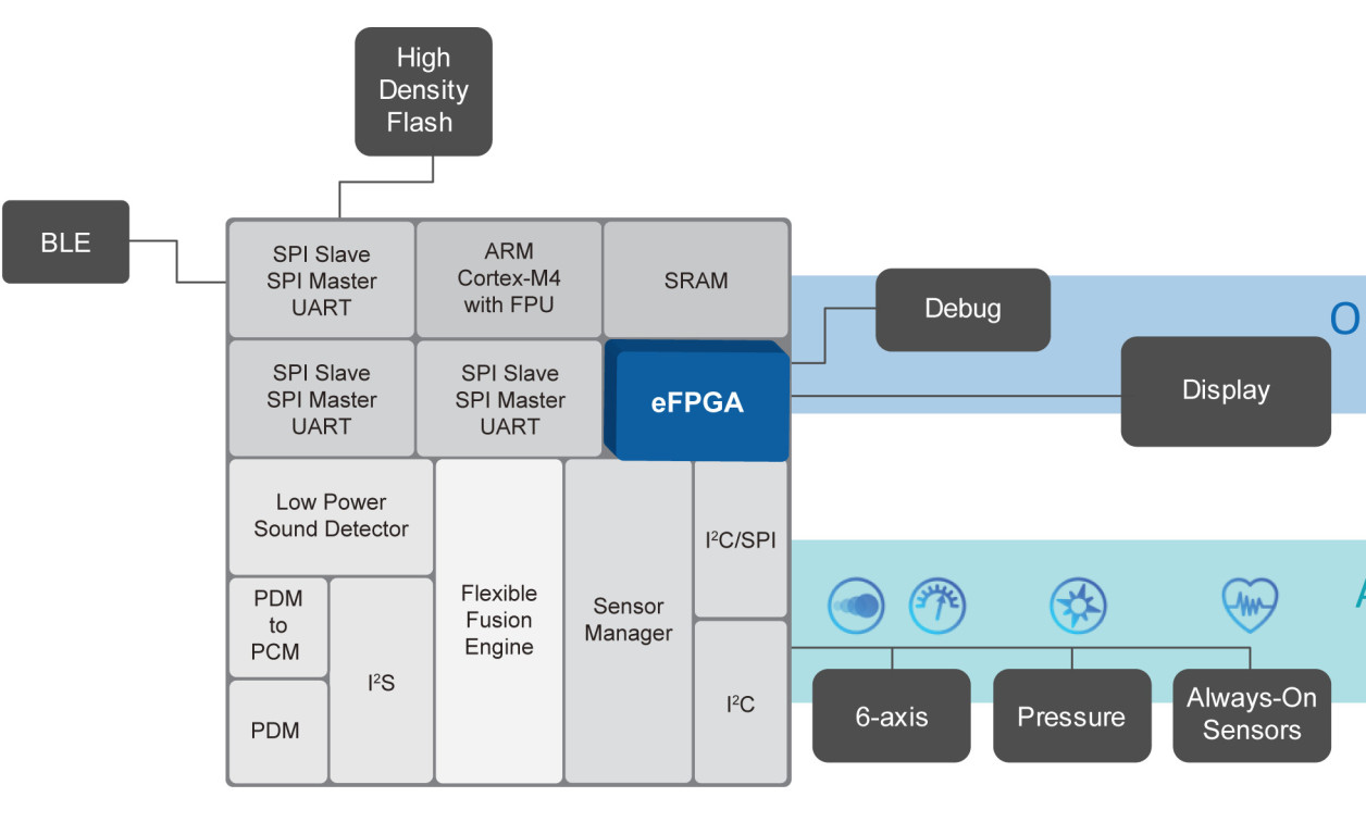
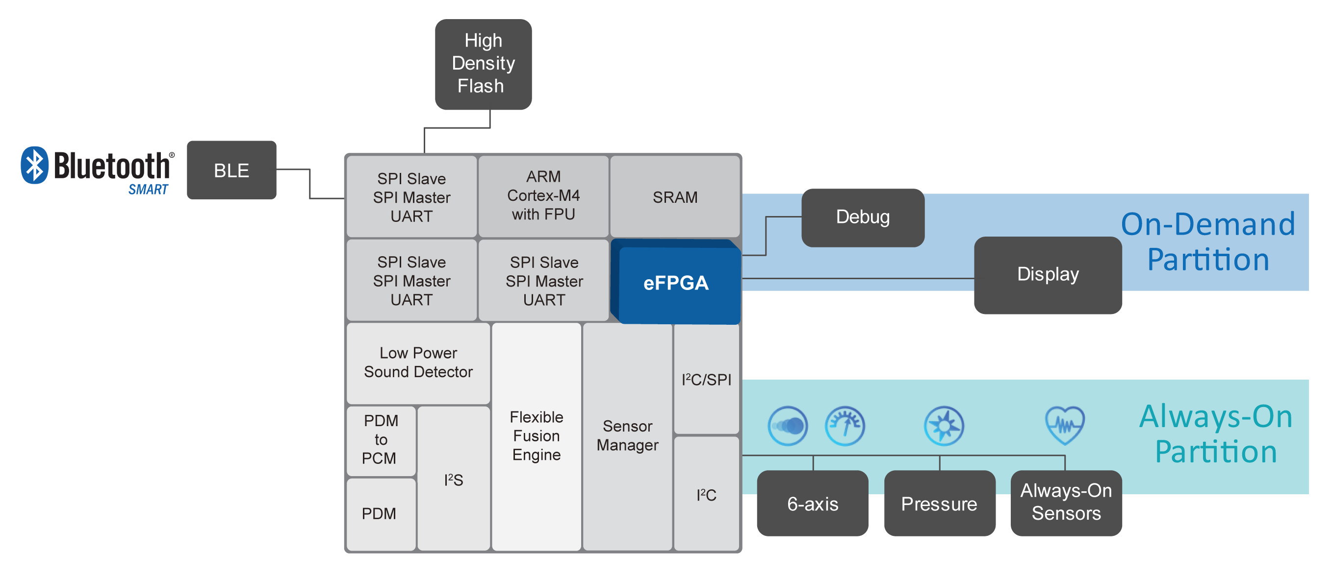
In some cases, experienced FPGA vendors also have learned how to effectively integrate eFPGA technology into their own SoC devices, which has allowed them to further refine their eFPGA IP offering by acting as their own customer for the technology. For example, QuickLogic has developed a sensor processing SoC for hearable, wearable, and IoT applications (Figure 1). This device includes eFPGA technology as the company has learned that having a programmable block of logic enables their customers to quickly implement new sensor processing algorithms and interface standards.
As users of the eFPGA tools themselves, QuickLogic engineers quickly learned what tools they needed and how to best optimize the eFPGA implementation design flow. Along the way, they encountered various issues and resolved them, ultimately creating the complete suite of tools and design files necessary for successful eFPGA IP integration.
Some of the files generated by these tools include the device wrapper file, back annotation files, and layout data. The device wrapper file is a netlist which defines the eFPGA “black box” ports and how they are connected to the rest of the SoC design. The back annotation files provide library and timing information that are critical to the design verification process. The layout data includes the physical layout information which the design team can use to instantiate the physical design blocks.
Uses of eFPGA in AI, IoT, security and other applications
SoCs are obviously used for a wide range of applications, and adding embedded FPGA technology only expands the potential set of use cases. However, there are some examples of applications in which SoC-with-eFPGA solutions offer particularly significant advantages over traditional SoCs.
We have already reviewed sensor processing, in which the embedded FPGA portion of the EOS S3 SoC enables rapid sensor algorithm and interface updates to be implemented without having to tape out a new version of the device. Voice processing with associated cloud-base AI is the next big step forward in human-machine interaction and having the ability to quickly and easily add new trigger words for ecosystems supporting “smart speaker” products such as Amazon’s Alexa.
The highly fragmented IoT market is another good example of where eFPGA technology can provide a substantial benefit. The overall market is huge, but few individual applications will have high volume market demand on their own. Thus, it makes sense for an SoC designer to employ a platform-based approach whereby their “base” device implements all the functionality each application has in common. Then the eFPGA technology can be used to quickly and cost-effectively create multiple product variants to address specific applications. New applications that suddenly appear can also be addressed without the time and cost associated with redesigning an ASIC.
Nearly any machine learning application including big data and deep learning can take advantage of the reconfigurable nature afforded by most eFPGA solutions. Hardware in the eFPGA block can be configured and then reconfigured as often as necessary to cheaply and efficiently solve some of the most complex problems addressed by computers today.
Another good example, and one especially relevant now, is the need to constantly update hardware-based security algorithms. As new security vulnerabilities or breaches are identified, delivering an updated defensive solution becomes time critical – a perfect fit for the eFPGA hardware in an SoC.
The future of eFPGA technology
Given that the development and unit cost trends will make embedded FPGA technology ever more attractive to SoC design teams, the future of eFPGA IP is extremely bright. As with every complex technology, though, there are some challenges. Among these is that one size does not fit all and there are many, many possible combinations of eFPGA IP architectures, sizes, and technologies along with SoC implementations across different foundries and process nodes. There are also potential integration issues associated with the need for differing numbers of metal layers, managing clock domain boundaries, and coordinating different power management schemes.
Even though eFPGA technology has been available in various forms for some time now, the market is just now moving from the early adoption phase to the mainstream phase. This trend will only accelerate in the near term. Example applications and end products are becoming easier to find and range from mobile devices, hearables, wearables and IoT to big data and communication centers to reconfigurable computing platforms, to cloud-based artificial intelligence.
However, eFPGA technology will be successful only when the programmable logic is integrated efficiently within the SoC. That requires the right combination of technology, architecture, and software tools so that the development teams have a complete and effective design flow enabling them to move seamlessly from concept to working silicon to post-manufacturing market-tuned and ready-to-ship product.


