
GOWIN Adopts HyperBus Interface for Internal PSRAM, External HyperRAM
May 04, 2019
News
HyperBus provides efficient use of package pins for high-speed interfacing with low pin count external memories, as well as internal PSRAM on GOWIN programmable devices.
SAN JOSE, CA and GUANGZHOU, CHINA. GOWIN Semiconductor Corporation now supports the HyperBus interface specification in their FPGA and programmable SoC solutions. HyperBus provides efficient use of package pins for high-speed interfacing with low pin count external memories, as well as internal PSRAM on GOWIN programmable devices. This helps reduce power, cost, and PCB footprint compared to legacy memory interface technologies.
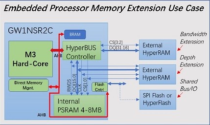
The HyperBus interface consumes only 11 pins. Additional memories can be multiplexed with an additional chip select. Using GOWIN’s HyperBus Memory Interface IP core, processors can directly access up to 64 Mb of PSRAM over configurable 8-16-bit DDR bus widths, while external HyperRAM and HyperFLASH memories can also be connected.
GOWIN HyperBus Memory Interface, PSRAM, and Flash PSRAM devices are in production now. For more information visit www.gowinsemi.com/en/support/ip_detail/15.


