
The Fundamentals of Transimpedance Amplifiers
September 23, 2019
Blog

The TIA circuit seems to be reasonably straightforward, so why all the hubbub over a circuit that has four components: a photodiode, an amplifier, a feedback resistor, and a feedback capacitor?
I’m surprised how often transimpedance amplifiers (TIA) and associated circuits keep coming back into our analog designers’ conversations. Medical photosensing applications demand a high level of analog precision and accuracy. These medical photosensing techniques are now merging into the digital domain with automotive and industrial LiDAR (light detection and ranging), security, brightness control and agriculture weather management applications. Several circuits tackle the photosensing task; however, I am going to focus on the basics. The primary analog photosensing or the TIA circuit provides a wealth of information that will carry through to your next light-sensing circuit design.
Precision TIA Circuits
The TIA circuit seems to be reasonably straightforward, so why all the hubbub over a circuit that has four components: a photodiode, an amplifier, a feedback resistor, and usually a feedback capacitor? With power connections, these circuits are ready to receive light and convert the impinging luminance to a usable voltage (Figure 1).
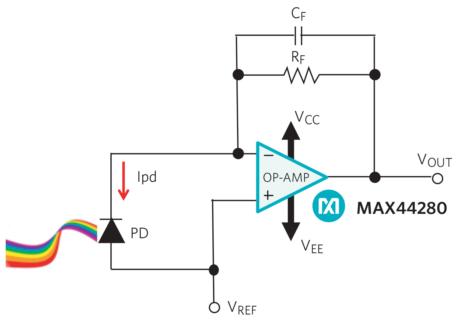
In Figure 1, the placement of the photodiode (PD) is across the inverting and noninverting inputs of the amplifier. In a dark environment, this forces the voltage across the diode to be 0V. Impinging light on the photodiode generates a current from anode to cathode that appears as an increase in the op amp's output voltage (VOUT). Now, you might think that the photodiode’s current (Ipd) is going in the wrong direction. In Figure 1, the direction of Ipd is definitely against standard diode operation. Avoid the trap of changing the direction of Ipd. The light controls the flow of the photodiode's electrons and holes across their PN-junction, causing the current to conduct from the diode's cathode to anode. The photodiode's current increases with intensifying luminance.
In Figure 1, the op amp’s output voltage versus the PD’s current creates a noninverting response (Figure 2).

In Figure 2, the zero-biased TIA response has an increase in output voltage as the luminance on the photodiode increases. An increase in luminance causes an increase in photodiode output current.
There are essential issues to apply to this circuit when you ensure precision performance. The photodiode’s output current is dependent on the light intensity. You will find that the maximum photodiode’s output current is typically in the microamp (mA) region. On the other hand, if you’re sensing low luminance signals, the photodiode output current could be in the picoampere (pA) region. For these ranges, the analog blood-glucose meter or CAT scanner, for example, requires analog granularity across the entire amplifier output range.
The op amp is directly connected to the photodiode. Consequently, the amplifier’s input bias current level must be as low as possible. The CMOS or FET input amplifiers typically have input bias currents in the picoampere range. In Figure 1, the MAX44280 op amp has a maximum input bias current of 0.5pA.
Digital TIA circuits
Digital TIA circuits are designed for high-speed circuits and have a photodiode digital, on-off, and input signal (Figure 3).
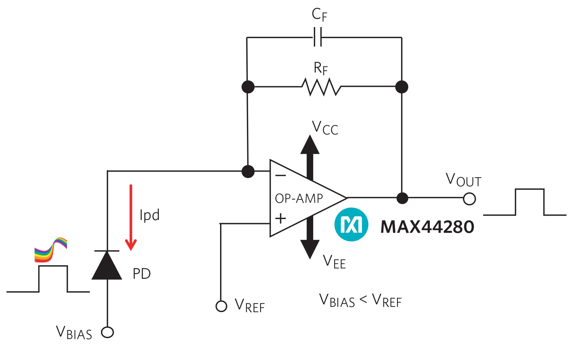
In Figure 3, the negative bias voltage across PD reduces the photodiode’s parasitic capacitance and also increases the photodiodes’ leakage current. This lower capacitance increases the speed of the TIA. However, there is always a side effect for improving any system performance. As you increase the TIA’s speed, you compromise the precision by creating PD leakage. But this is actually not a serious compromise because the pulsing signal now has the circuit performing in the digital domain, and digital noise margins easily tolerate the leakage current error.
In Figure 3, the op amp’s output voltage versus the PD’s current also creates a noninverting response (Figure 4).

In Figure 4, the negative reverse-biased TIA response has an increase in output voltage as the luminance on the photodiode increases, causing an increase in photodiode output current.
The photodiode is no longer connected directly across the op amp. The critical amplifier specifications are now input capacitance and bandwidth. In Figure 3, the MAX44280 op amp has a 0.4pF input capacitance and a 20MHz bandwidth.
Conclusion
The basic TIA design is for precision systems while a digital TIA design is for high-speed digital circuits. In this article, the critical op amp specifications are input bias current and high GBWPs. But this general overview is just a start.
In future blogs, I will delve into the details, nuances, and interactions between these four components (PD, op amp, R, and C). The next article will take a closer look at the photodiode.


