
JESD204C Primer: What's New and in it for You, Part 2
September 24, 2019
Blog

Since Part 1 laid a suitable foundation, let?s take a closer look at a few of the more notable new features of the JESD204C standard.Del Jones, Analog Devices
In Part 1 of the JESD204C primer series, the new version of the JESD204 standard was justified by describing some of the problems it solves. The differences between the B and C version of the standard were summarized by describing new terminology and features, then providing a layer-by-layer overview of these differences. Since Part 1 laid a suitable foundation, let’s take a closer look at a few of the more notable new features of the JESD204C standard.
The 64b/66b and 64b/80b Link Layers
For the 64b/66b link layer, the 66-bit block of data is two sync header bits followed by eight octets of sample data and is partially based on the block format defined in IEEE 802.3, clause 49. Unlike the IEEE standard, there is no encoding—the payload data are simply the converter sample data that have been packed into frames of data by the transport layer. Since there is no encoding to ensure a certain number of data transitions occur to provide dc balance, the sample data must be scrambled. These scrambled octets of framed data are placed directly into the link layer with the two sync header bits attached.
The 64b/66b block format is illustrated in Figure 1. The example shows the case where one lane of data consists of frames that contain one sample per frame from one converter. Block mapping rules are very similar to the frame mapping rules from the JESD204B standard. Mapping of octets into 64-bit blocks is done in order with D0 representing the first octet of a frame. For example, if F = 8, D0 represents the first octet of the JESD204C frame, and D7 represents the last octet of the JESD204C frame. The first octet of the frame is the octet whose MSB is the MSB of Sample0 of Converter0 (same as in JESD204B). For example, if F = 2, D0 and D1 represent the first frame, D2 and D3 represent the second frame, etc.
To remain consistent with the approach used in JESD204B, the octets within the multiblock are shifted into the scrambler/descrambler in the order of MSB to LSB.
For cases where E is 1, every multiblock starts on a frame boundary. If E > 1, the extended multiblock will (and must!) start on a frame boundary. This is covered more in the Multiblock (MB) and Extended Multiblock (EMB) section.
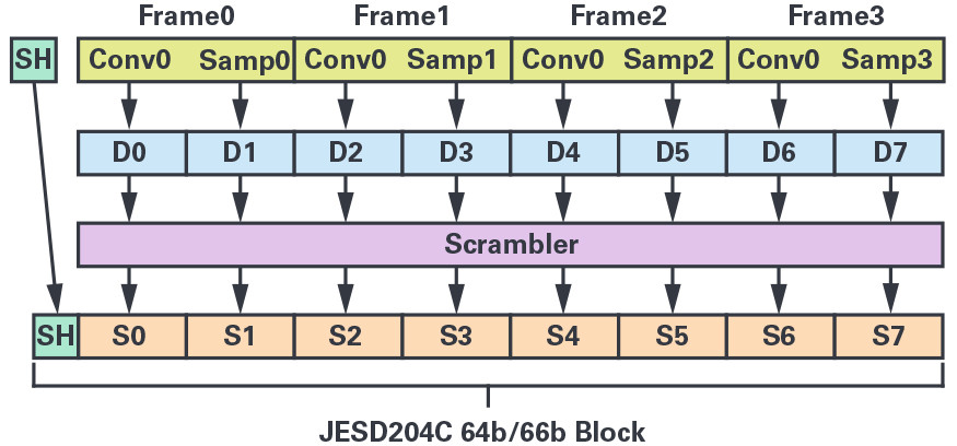
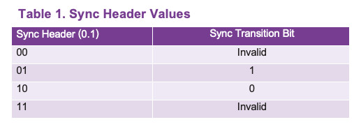
The sync header is a 2-bit unscrambled value at the beginning of each block, the contents of which are interpreted to decode a single sync transition bit. These bits must be either a 0-1 sequence to indicate a logic 1 or a 1-0 sequence to indicate a logic 0. Table 1 enumerates the sync header sync transition bit values.
The 64b/80b block format is illustrated in Figure 2. In addition to the eight octets of sample data and the two sync header bits, there are two fill bits placed in between each of the octets. The values of the fill bits are determined by a 17-bit PRBS sequence to reduce spurs and ensure an appropriate number of data transitions to maintain dc balance. The unscrambled fill bits are inserted into the block after the sample data has been scrambled.
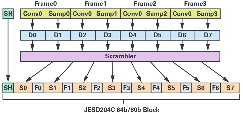
The 64b/80b option was provided to retain the same clock ratios as 8b/10b, which helps simplify the phase-locked loop (PLL) design while also minimizing spurs. This scheme would be preferred over 8b/10b in applications that want to use forward error correction or take advantage of the other functions provided by the sync word, which will be discussed shortly.
Multiblocks (MB) and Extended Multiblocks (EMB)
There are 32 blocks in a JESD204C multiblock. The 32 sync transition bits in each multiblock make up a 32-bit sync-word. These will be discussed in more detail later. An extended multiblock is a container of E multiblocks and must contain an integer number of frames. E > 1 is required when a multiframe does not contain an integer number of frames. The format of the multiblock and extended multiblock are illustrated in Figure 3.
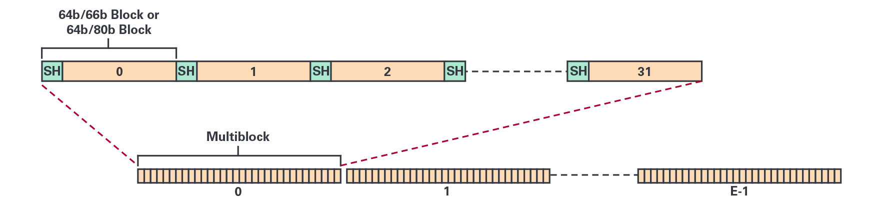
A multiblock is either 2112 (32×66) or 2560 (32×80) bits depending on which 64-bit encoding scheme is used. For most implementations and configurations, an extended multiblock will be just one multiblock. The E parameter is introduced in JESD204C and determines the number of multiblocks in the extended multiblock. The default value for E is 1. As implied above, E > 1 is required for configurations where the number of octets in the frame, F, is not a power of two. The equation for E is: E = LCM(F, 256)/256. These configurations are typically preferred when transmitting 12-bit samples and N’ is set to 12 to maximize bandwidth efficiency in the link. This requirement ensures that the EMB boundary coincides with a frame boundary.
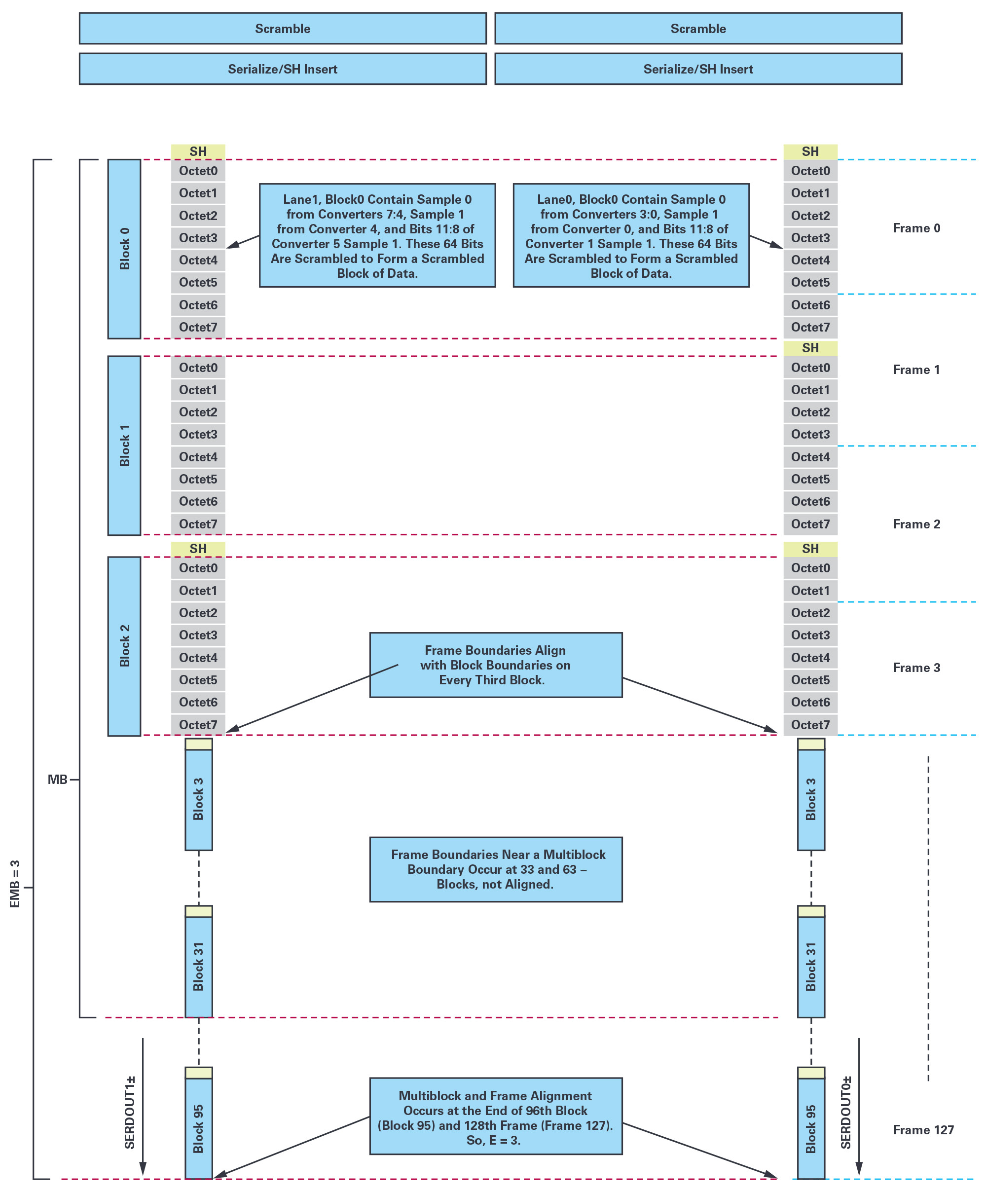
Figure 4 and Figure 5 illustrate an example of a JESD204C configuration where E > 1. The JESD204C configuration shown is for the case where LMFS = 2.8.6.1, N’ = 12, and E = 3. Figure 4 shows the transport layer mapping. In this configuration, there are four 12-bit samples per lane, which translates to six octets. Since each block of a multiblock needs eight octets, the block is filled in with two octets (1.33 samples) from the subsequent frame.
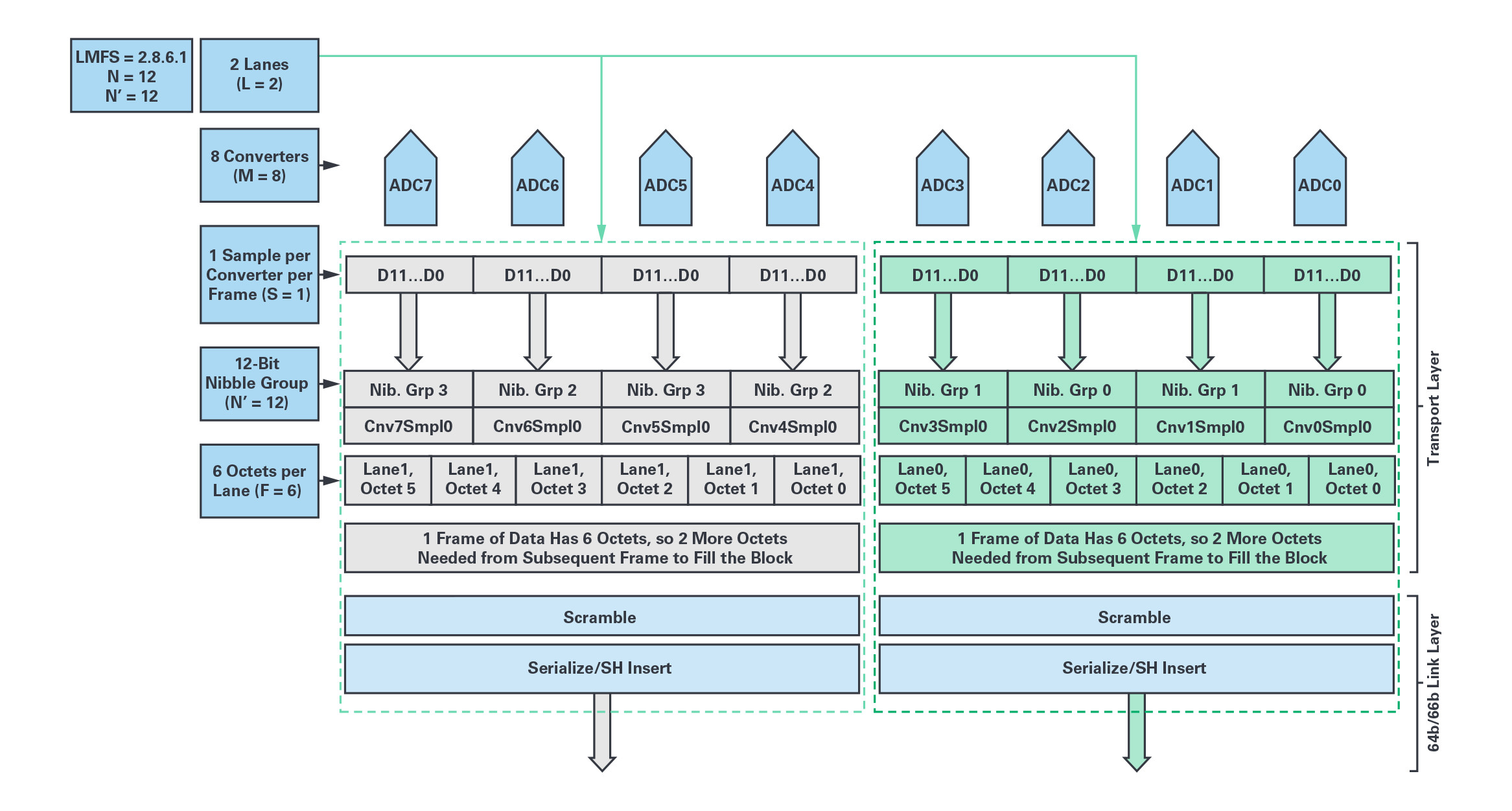
Figure 5 shows how the blocks and multiblocks are formed using the frames of data from the transport layer. As illustrated, you can see that frame boundaries align with block boundaries on every third block. Since multiblocks consist of 32 blocks, frame alignment to a multiblock is not achieved until after the third multiblock. Therefore, E = 3.
LEMC is the extended multiblock counter and is roughly equivalent to the LMFC in the 8b/10b link layer. SYSREF aligns all LEMCs in a system and the LEMC boundaries are used to determine synchronization and lane alignment.
Sync Word
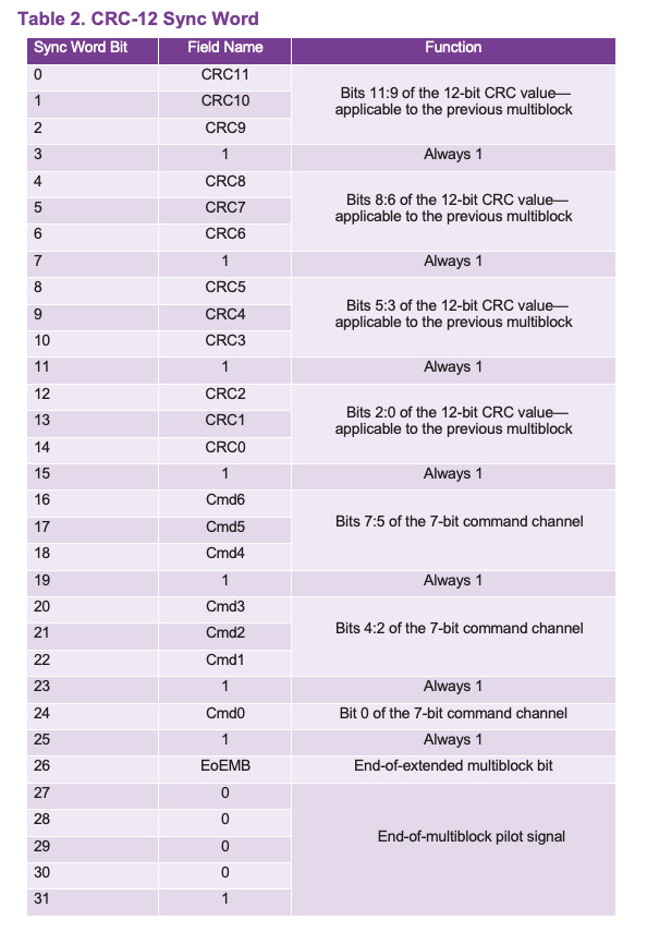
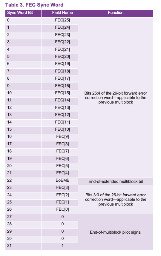
The 32-bit sync word is made from each of the sample headers from the 32 blocks within the multiblock where bit 0 is transmitted first. The sync word is used to provide lane synchronization and enable deterministic latency. In addition, it can optionally provide for CRC error checking, forward error correction, or provide a command channel for the transmitter to communicate to the receiver.
There are three different formatting options for the 32-bit sync word. In each case, the end-of-multiblock sequence is required since it is used to acquire multiblock synchronization and lane alignment. Table 2 and Table 3 show the different bit fields available in the two most common use cases.
64b/66b Link Operation
The link establishment process when using the 64b/66b link layer starts with sync header alignment, then progresses to extended multiblock synchronization, and finally to extended multiblock alignment.
Sync Header Alignment
The sync transition bit in the sync header ensures that there is a data transition at every block boundary (66 bits). A state machine in the JESD204C receiver detects a data transition and then looks for another transition 66 bits later. If the state machine detects bit transitions at 66-bit intervals for 64 consecutive blocks, sync header lock (SH_lock) is achieved. The machine is restarted if 64 consecutive transitions are not detected.
Extended Multiblock Sync
Once sync header alignment is achieved, the receiver looks for the end-of-extended-multiblock (EoEMB) sequence (100001) in the transition bits. The structure of the sync word ensures that this sequence can only happen at the appropriate time. Once an EoEMB is identified, the state machine examines every 32nd sync word to ensure the end-of-multiblock pilot signal (00001) is present. If E = 1, the EoEMB bit will also be present with the pilot signal. If E > 1, then every E × 32 transition bits, the pilot signal will have included the EoEMB bit. Once four consecutive valid sequences are detected, then end-of-extended-multiblock lock (EMB_LOCK) is achieved. Monitoring of every E × 32 transition bit continues and EMB_LOCK is lost if a valid sequence is not detected and the alignment process is reset.
Extended Multiblock (Lane) Alignment
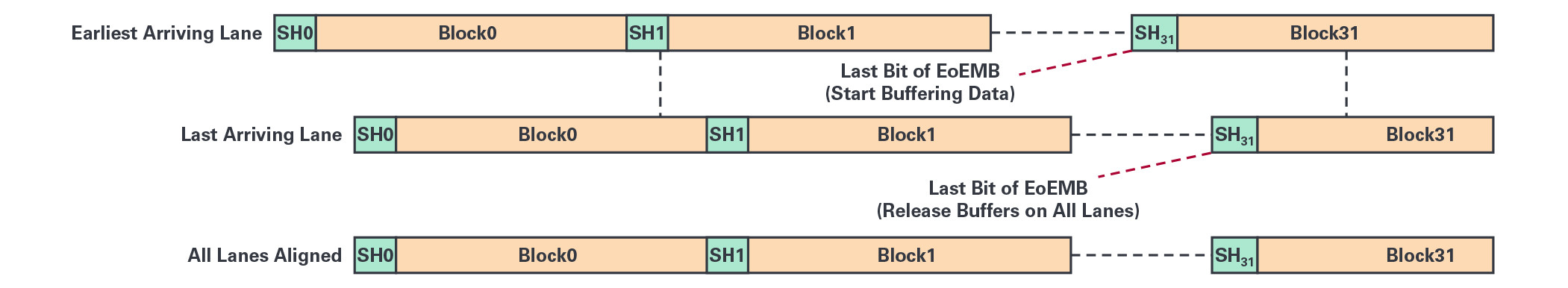
Lane alignment when using the 64b/66b link layer is very similar to when using the 8b/10b link layer in that an elastic buffer is employed in the JESD204C receiver on each lane to store incoming data. This is called extended multiblock alignment and the buffers begin storing data at the EoEMB boundary (rather than the /K/ to /R/ boundary during ILAS when using the 8b/10b link layer). Figure 6 illustrates how lane alignment is achieved. Each lane’s receive buffer starts buffering data once the last bit of the EoEMB is received except for the last arriving lane. When the last arriving lane’s EoEMB is received, it triggers the release of all the lane’s receive buffers so that all lanes are now aligned.
Error Monitoring and Forward Error Correction
JESD204C sync word options give the user the ability to either monitor or correct errors that may occur in the JESD204 data transmission. The trade-off associated with error correction is additional latency in the system. For most applications, error monitoring using the CRC-12 sync word is suitable since it provides for a bit-error rate (BER) of greater than 1 × 10–15.
The CRC-12 encoder in the JESD204C transmitter takes in the scrambled data bits of each multiblock and computes 12 parity bits. These parity bits are transmitted to the receiver during the subsequent multiblock. The receiver will likewise compute 12 parity bits from each multiblock of data it receives, and these bits are compared to those that were received in the sync word. If all the parity bits do not match, there is at least one error in the received data and an error flag can be raised.
For error-sensitive applications that are not sensitive to added latency (like test and measurement equipment), using FEC can result in a BER of better than 10 × 10–24. The FEC circuit in the JESD204C transmitter computes the FEC parity bits of the scrambled data bits in a multiblock and encodes these parity bits on the sync header stream of the next multiblock. The receiver calculates the syndrome of the received bits, which is the difference between the locally generated and the received parity. If the syndrome is zero, the received data bits are assumed to be correct. If the syndrome is non-zero, it can be used to determine the most likely error.
The FEC parity bits are calculated in a similar way to CRC. The FEC encoder takes in the 2048 scrambled data bits of the multiblock and adds 26 parity bits to construct a shortened binary cyclic code. The generator polynomial for this code is:

Final Thoughts
To meet the faster data processing demands for data-intensive applications over the course of the next several years, JESD204C defines the multigigabit interface as a required communications channel between data converters and logic devices. The up-to 32 GSPS lane rates and 64b/66b encoding enables ultrahigh bandwidth applications with minimal overhead to improve system efficiency. 5G communications, radar, and electronic warfare applications all stand to benefit from these and other improvements in the standard. With the addition of error correction, cutting-edge instrumentation and other applications can count on operating without error for many years.
For more information on JESD204 and its implementation in Analog Devices products, please visit ADI’s JESD204 serial interface page. For more information on ADI high speed converters, visit our RF converters page and 28 nm RF data converter page. For more information on ADI’s transceiver products, visit our RadioVerse™ page.
About the Author
Del Jones is an applications engineer for the High Speed Converters Team in Greensboro, North Carolina. He has worked for ADI since 2000, supporting ADCs, DACs, and serial interfaces. Prior to ADI, he worked as a board and FPGA design engineer in the telecommunications industry. Del earned his bachelor’s degree in electrical engineering from the University of Texas at Dallas.


