
Designing small, dense layouts for medical electronics products
January 01, 2008

The complexity of compact medical electronic devices substantially increases PCB layer count because of increased product functionality.
As electronics technologies advance rapidly and demand for portable products increases, carry-along medical instruments and compact and wireless devices are becoming more prevalent in hospitals, health care centers, and first responder vehicles. Small form factor products like these are based on compact PCBs with tightly spaced digital and analog circuits placed directly next to each other.
The complexity of compact medical electronic devices substantially increases PCB layer count because of increased product functionality. With advances in technology, these small devices now perform considerably more electronic functions than their desktop predecessors. Consequently, the number of layers is increasing to perform signal routing, among other functions. Newer compact medical devices generally require PCBs that comprise 10-12 PCB layers, sometimes more.
Devices shrinking
Layers and routing get more complicated as device sizes decrease. Active devices are shrinking in size and come packaged in advanced packaging, such as Ball Grid Array (BGA), Quad Flat Pack (QFP), and Chip Scale Packaging (CSP), adding to the complexity and difficulties associated with small form factor PCBs. More fine-pitch BGAs are being used in compact medical devices. MicroBGA devices range from 0.5 mm pitch down to 0.3 mm, making assembly procedures extremely challenging.
Passive devices such as resistors and capacitors are also shrinking. Five years ago, 1206 and 0805 package types were used frequently. Today’s 0402 and 0201 packages are half to quarter the physical size of those earlier device packages. These smaller packages enable smaller layouts, but make assembly difficult and require considerable precision through expensive, pick-and-place, surface-mount lines and other ancillary rework stations.
First-pass yields expectations
Considering the total number of daunting product challenges, the PCB design, fabrication, and assembly process becomes highly complex. Therefore, the prudent medical electronics OEM must carefully review first-pass yields to determine how many products are passing. Likewise, the Electronic Manufacturing Services (EMS) provider team must embrace the mantra of doing the design, fabrication, and assembly right the first time.
First-pass yields are more important to the design and assembly of compact medical electronic devices for the simple reason that they are more difficult to manufacture and rework than larger products. The first-pass yields process is conducted when assembly and testing are completed. Test coverage is evaluated to determine failure rates and failure analysis is performed. First-pass yields must ensure that a correct thermal profile is created and applied, component polarities are accurate, missing or wrong components are not used, adequate solder paste is dispensed, and correct flux is used.
Typically, first-pass yields should be 75 percent or higher at prototype levels. However, when life-critical products are involved, medical OEMs require 90 percent first-pass yields. This means the experienced EMS provider must have a process in place to periodically review design and assembly data and make the necessary improvements to create great first-pass yields of 90 percent or higher.
The first-pass yields metric indicates how tight an EMS provider’s design and assembly procedures are and how efficiently the checks and balances are put into place to ensure product reliability.
Design considerations
Design For Assembly (DFA) for medical products relies heavily on multiple team interaction. Design, fabrication, assembly, and component procurement teams assigned to a given PCB project must precisely tune into a project’s specifications. Design engineers must be fully aware of certain assembly aspects, and likewise, assembly engineers must understand a project’s design intricacies in detail, such as automated placement and inspection issues and rework requirements.
These teams working together can address and resolve most of the issues and questions at root cause levels. For example, if a design team specifies a component with extended lead times of 12 weeks or more, the procurement team can flag this issue and suggest a readily available replacement component.
Efficient DFA calls for the following considerations to be addressed:
|
|

- Adequate test points should be deployed at the PCB layout stage across the board to allow complete access and coverage during flying probe or ICT test or for direct probing. Figure 1 shows a board with adequate test points being tested at the flying probe testing stage. Medical device testing requires multiple, redundant test points to capture data precisely. The test engineer checks this coverage by accessing two or three test node points, if needed.
- When fabricating a board, it is important to consider panelization versus fabricating one board at a time. This is especially true when the board size is relatively smaller, such as 30 square inches or less. This panelization such as shown in Figure 2 increases fabrication and assembly speed, thereby reducing OEM costs.
- While placing components at the layout stage, it is prudent to use one side of the board versus utilizing both sides, if possible. Using components on only one side reduces nonrecurring engineering costs at assembly and test stages. It also speeds up component placement at pick-and-place machines and reduces component testing time at ICT or flying probes, thus saving OEMs money and time. Placing components only on the top side also reduces rework, quality control, and debug times, all of which can reduce assembly costs.
- All mechanical considerations should be kept in mind at PCB design stages for DFA considerations, such as designing at least two, if not three mounting holes for the PCB. Also, fiducial marks for each of the active components should be designed, and polarity on polarized components should be clearly defined on the silk screen on the board. This practice eliminates confusion that may arise at component placement, testing, and debugging stages, thereby reducing production costs.
|
|

Attention to more details
Hardware engineers specifying components at design stages should use time-tested and verified components as much as possible. Using these components reduces debug and test times and makes a medical product more reliable and predictable. Effective DFA also calls for using commonly available components with specifications and features already proven time after time in multitudes of other system applications.
Another major consideration involves careful monitoring of equipment-related features and physical tolerances. Take for example drill machines used for drilling holes during the PCB fabrication process of a medical product. A drill bit that drills into a PCB can meander or wander. DFA demands that tight tolerances be maintained in this regard, especially if smaller hole sizes are designed in, say 8 mils or less. Also, it is crucial to maintain proper alignment of multiple symmetrical components. If modular designs are involved, it is important to keep all modules alike so that when an IC is placed in one module, similar ICs are identically placed in the second, third, fourth, and subsequent numbered modules. This is especially important for a small and densely populated medical product.
In the same way, resistor and capacitor networks must be similarly placed to reduce SMT machine programming and placement time. In some cases, a PCB may be odd-sized or shaped. Hence, this particular feature is made clear at the outset in DFA so that when the required fixture is used in the assembly process, its limitations are specified up front to make the assembly process smooth, more predictable, and efficient.
Lastly, detailed documentation in terms of design, fabrication, and assembly notes is a vital aspect of DFA. This disciplined procedure assures that all elements of a design are properly executed during fabrication and assembly. Well-prepared notes are especially crucial if multiple vendors are involved; design layout may be performed by one company, PCB fabrication by another, with a third company doing the assembly stages, and a fourth performing rework and test.
Mixed signal designs
To address DFA issues for mixed signal designs on a compact medical product, a well-defined and clear-cut strategy should be identified to:
- Reduce signal-to-noise ratios
- Properly define power and ground signals and planes according to component placement
- Shield high-speed digital signals from analog segments
If these DFA strategies are not incorporated at layout, a product could create unacceptable noise levels and require redesign, costing more time, resources, and money.
Each mixed signal board design is different and demands interactive design negotiations between expert mixed signal designers and the compact medical device OEM. When designing mixed signal components on a PCB layout, certain considerations are critical to achieving optimum performance.
Mixed signal design is difficult because analog devices possess different characteristics compared to digital components, such as different power ratings, current and voltage callouts, heat dissipation requirements, and signal speeds. Consequently, it is important to recognize certain problematic areas and then implement the solutions correctly in a mixed signal medical design.
Bad, better, best layout
|
|

Mixed signal circuitry PCB placement is among the more crucial DFA points. First, observe the wrong method. As shown in Figure 3a, a separation exists in the middle between the analog and digital ground planes, appearing as an L- or S-shaped figure, with traces crossing that separation. This is a poor layout because the trace discontinuity in the plane separation and the lack of a return path cause noise and cross talks.
What is missing is a respective solid plane located underneath the trace to allow for continuous impedance on that trace. Also, the trace crossover from the analog to the digital plane prevents a good return path for these particular traces. A good DFA design should maintain a distinct separation of split planes between the analog and digital ground planes as well as keep analog traces under the analog split plane and digital traces under the digital split plane. Otherwise, noise is created on the board and signals deteriorate.
Ideally, the analog section of a board must be totally isolated in terms of placement, routing, and plane creation. Plus, analog traces should only run underneath their analog reference power or ground plane. Conversely, digital traces should run under the digital section with respective power and ground planes, such as in Figure 3b. This keeps impedance constant and provides a good return path for signals.
However, there are cases in which a complete analog and digital separation is not possible because of mechanical and/or space constraints on PCB real estate. The best approach here is to run analog and digital traces on separate layers. If there is no plane separation between the layers, the rule of thumb is to run them perpendicular to maintain signal authenticity. But they should never run parallel to each other.
|
|

Figure 3c shows the best placement method using an Analog-to-Digital Converter (ADC) IC as an example. One side of the IC has analog pins resting right on top of the analog plane, while the other side has digital pins placed squarely on the digital plane.
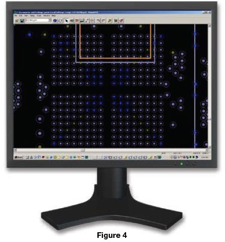
When separation isn’t as exact and ideal as this ADC IC example, mixed signal circuitry separation at the device level requires careful design techniques. Take for example a mixed signal device packaged in a BGA. Figure 4 shows proper separation between analog and digital sections. Analog and digital circuitry in the device is isolated with about a 15 mils wide gap so that all analog signals and traces are on the analog side and their counterpart digital sections are on the digital side.
|
|
Robust designs
The demands for greater robustness, high quality, increased reliability, and better yields are all associated with compact medical electronic devices. ISO standards such as ISO 9001:2000 and ISO 13485 provide EMS companies the extra qualifications to comply with these demands and allow them to assure high standards of product quality to medical product OEMs. These ISO standards are not required for product manufacturing; however, they can provide a medical device OEM greater assurance of product quality and reliability.
While following these standards is important, going beyond the standards by paying attention to the details of the DFA process makes the ultimate difference in the success of a compact device design. A rigorous DFA approach can save costs and space, resulting in a robust PCB design for life-critical products.
Zulki Khan is founder and CEO of NexLogic Technologies, Inc., based in San Jose. Prior to NexLogic, Zulki was general manager for Imagineering, Inc. He has worked on high-speed PCB designs with signal integrity analysis and contributed numerous articles to EMS industry publications. Zulki holds a BSEE from NED University of Engineering and Technology in Karachi, Pakistan and an MBA from the University of Iowa.
NexLogic Technologies
408-436-8150 ext. 102
[email protected]
www.nexlogic.com


