
Fail-Safe Data Storage for IoT Applications
November 05, 2018
Blog

With the advent of the IoT, every device in the field can begin communicating over the network. A conservative estimate predicts that over 10 billion devices will be connected by the year 2020.
For decades, the basic architecture of remote sensing nodes consisted of a controller, sensor, local storage memory, network connectivity interface and battery. This architecture has been replicated in all the systems that interact with real world inputs. In an industrial automation system, controllers monitor several sensors at varying rates, store time-stamped sensor data in local memory or expansion memory, and transfer data via industry standard buses like ProfiBus, etc. For an automotive ADAS system or an Event Data Recorder (EDR) system, several MCUs are simultaneously collecting and controlling the electronics of the car for a better driving experience and fail-safe data logging. A medical system requires similar functionality for life-critical sensor data that either get recorded locally or uploaded periodically to a central network.
All these systems are trying to solve the fundamental problem of collecting data, storing critical parts of it, and taking appropriate action based on data analytics. However, they all have different priorities. Industrial systems tend to capture massive amounts of data in short intervals from a wide variety of sensors and must maintain a detailed log locally as well as remotely. An automotive system might generate data at a slower rate, but data retention is critical, and, in some cases, data loss can be life threatening. Since most cars tend to run for over a decade, the long-term reliability of storage tends to be a critical criterion when selecting the appropriate memory. Portable medical systems, on the other hand, tend to prioritize power consumption when selecting the optimal memory technology. Medical implants or hearing aids are highly optimized to store data accurately while consuming the lowest power possible, as these systems operate on a battery supply. Designing fail-safe data storage, with long-term reliability and low power consumption, is one of the critical challenges facing the designers of medical systems.
With the advent of the Internet of Things (IoT), every device in the field can begin communicating over the network. A conservative estimate predicts that over 10 billion devices will be connected by the year 2020. These include cars, industrial automation equipment, medical implants, and new age devices like wearables, smart homes, etc. Next-generation 5G networks are already being deployed in several parts of the world and are expected to handle a majority of the traffic coming from these devices. But there are several unanswered questions that data scientists and system designers are trying to address today.
- Which devices need to be connected to the cloud?
- How much information needs to be broadcasted?
- How much processing can be done locally?
- Who pays for the cloud?
A trivial approach is to upload everything to the cloud and handle processing remotely. While this may work for smaller and isolated systems, once the world becomes more connected and a plethora of systems are trying to upload information, we’ll need to consider the cost of network versus local storage and processing. An autonomous car can generate several gigabytes of data per hour while driving. To anticipate future demand, now is the time to decide what to transfer and what to store locally for compressed transfer later. The same problem will be faced by industrial and medical system designers. Industry 4.0 is already migrating from “upload everything to the cloud” to a “process locally and upload smartly” approach. This makes choosing the optimal local data storage relevant for future systems.
These systems will need reliable, low power, fail-safe memories for storing critical data. One approach is to use available Flash memory to log data. Flash technology is designed for efficient read operations and hence it has become ubiquitous for boot code and firmware storage. As Flash is already available to the system, designers may make the easy choice to use a Flash for data logging without understanding the technology limitations of Flash when it comes to performing write operations. A Flash cell can be “programmed” to contain new data only if the cell is erased beforehand. Programming a cell allows a change from logic ‘1’ state to logic ‘0.’ During the next update, if the cells need to hold a logic ‘1,’ the cell must first be erased.
To optimize erase speed and program times, Flash manufacturers have created different page, block, and sector architectures. A page is the smallest quantum of data that can be programmed into the Flash at one time. Flash devices contain an internal page size buffer that allows for temporary storage of data. Once the transfer from the external interface is complete, the device initiates a page program operation on a page that is already erased in the main array. If this page contains old data, then it must be erased prior to a program operation. Every time an erase is performed, the Flash cell deteriorates. This phenomenon is quantified as endurance in a Flash datasheet. Typically, the best Flash devices are rated for endurance cycling of 100,000 erase-program cycles and are no longer guaranteed to reliably store data after reaching this limit. While this number appears large on paper, we will demonstrate that this device endurance falls short quickly even in low-end data logging systems.
Some manufacturers implement byte programming and delayed programming from buffer to Flash memory. While these features do simplify the program operation into the device, they do not alleviate the Flash devices from the underlying technology limitation of endurance. To compensate for these limitations, the system designer is forced to implement a complex file system to handle wear leveling of Flash cells (i.e., spread wear evenly throughout the cells). The software overhead of a file system slows down the system.
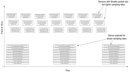
Let us evaluate scenarios where designers may consider a Flash-based memory for data logging. In industrial automation and asset management systems, sensor nodes tend to capture data several times per second, periodically sampling several different kinds of sensors. The node then assembles the packets for a network upload. Typically, these data packets can range from 16 bytes to 128 bytes. As there is always a risk of power failure, these packets are stored on a non-volatile memory to avoid data loss. Vibration sensors or stepper motor position sensors provide short bursts of data every few milliseconds while sensors like temperature or humidity provide data once every second, but the logged data packet is comprised of data from several sensors.
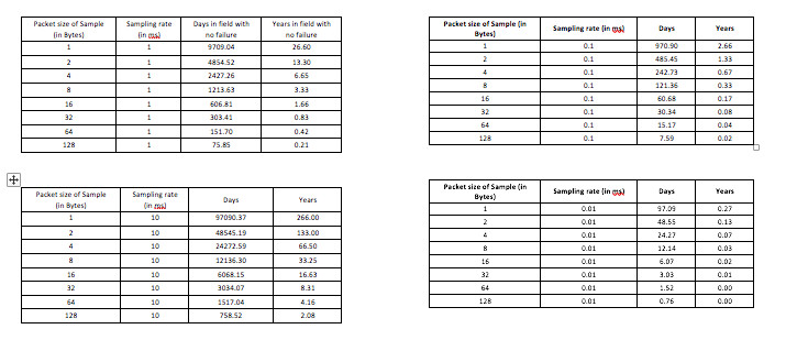
The tables below provide a comparative analysis of packet size versus sampling rate and how it wears down
a Flash memory if it is used for datalogging. This example uses an 8Mbyte of Flash with 10^5 endurance cycles.
The following graphs provide an interpretation of this data. We observe that for a low-end system, logging 8-16 bytes of data every 1 ms, an 8 Mbyte Flash wears out in under five years. An automotive or an industrial system is expected to be in field for over a decade.
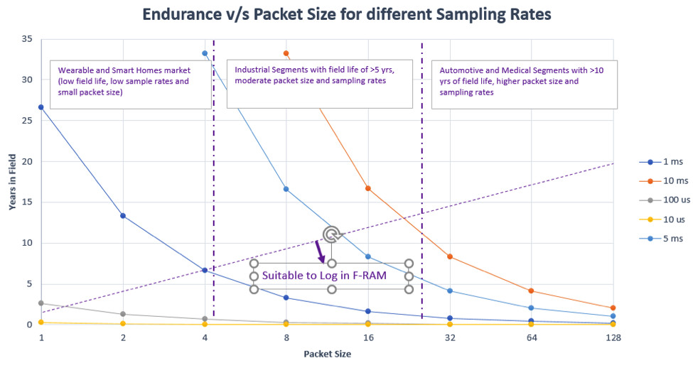
A low cost, high-risk option of simply adding more Flash memory requires a complex file system to handle wear leveling in Flash devices. If a file system is not implemented, then the system needs to handle the periodic chip erase cycles once the whole memory is rolled over. This problem only gets aggravated in today’s IoT world with ever-increasing data collecting terminals. Flash-based memories are well-suited for boot code and firmware storage, where the number of write cycles don’t exceed more than 1,000 throughout the lifetime of the product in field.
An ideal approach to address the data-logging problem would be to use a high endurance, instantly non-volatile memory, which does not put data at risk due to program and erase delays. Ferroelectric RAMs (FRAM) are suited to address these kinds of applications. FRAM offers endurance cycles of 10^14 cycles, has instant non-volatility, and does not require program and erase operations. Any data that have entered the device interface is instantly stored. To put this in context, a 4-Mbit FRAM can log 128-byte data packet streams every 10us and not wear out for over a thousand years.
FRAM memory cells consume power only when they are being written or read, so standby power consumption is on the order of a few microAmperes. This makes it feasible to operate FRAM memories in devices that run on batteries. Hearing aids and high-end medical wearables designed to sample heartbeats are examples of power-sensitive applications where FRAM can provide the low power and high endurance performance required. In automotive systems, where data are continuously logged into memory, a Flash-based system will fail to capture data during the “program” periods of Flash. In contrast, FRAM-based logging offers high reliability for these systems.
The high endurance, ultra-low power consumption, and instant non-volatility of FRAM make it compelling alternative memory for critical data logging in the connected world. Today, FRAM memories are available for specific markets like Automotive and Industrial. FRAM also supports SPI, I2C, and parallel interfaces with densities ranging from 4 Kbits to 4 Mbits. For more details on designing fail-safe data storage for IoT applications, see Interfacing FRAM using SPI and Designing an FRAM Data Logger.
Nilesh Badodekar is an Applications Engineer at Cypress Semiconductor. He has a master’s degree in Visual Information Processing and Embedded Systems from Indian Institute of Technology, Kharagpur, India.


