
Designing Smart Home and Wearables IoT Applications ? Part II
September 11, 2018
Story

Watches are no longer just for telling time. Smart watches have turned our wrists into smart phone holsters by enabling text messaging, phone calls, and health monitoring.
In part I of this article series, we covered IoT market trends, the relevance of smart home and wearable applications, and showed an example implementation of a smart home door lock controller. In part II, we’ll explore the implementation of a wearables application.
Watches are no longer just for telling time. Smart watches have turned our wrists into smart phone holsters by enabling text messaging, phone calls, and health monitoring. A wearable is a wireless device “almost always” worn by the user. For example, a fitness monitor is a wearable device that can keep track of a person’s fitness by monitoring parameters like heart rate, exercise, sleeping habits, body temperature, perspiration, etc. These devices have multiple sensors and can usually communicate to a device connected to the internet like a smart phone or a PC. These devices have three primary features:
- Always on: Because fitness monitors are operating continuously, these devices require long battery life. One of the great challenges when designing wearables is that they are power hungry and are often limited in the size of battery they can hold.
- Monitor Activities: A fitness monitor senses, processes, logs, and reports user activities. This includes monitoring multiple sensors and performing “sensor fusion” where data from multiple sensors are correlated using a DSP-like engine to analyze more complex behaviors and track them in a way users can understand and use.
- Exchange data: This includes ability to communicate collected and analyzed information to other devices, such as sending notifications and alerts to/from smart phones.
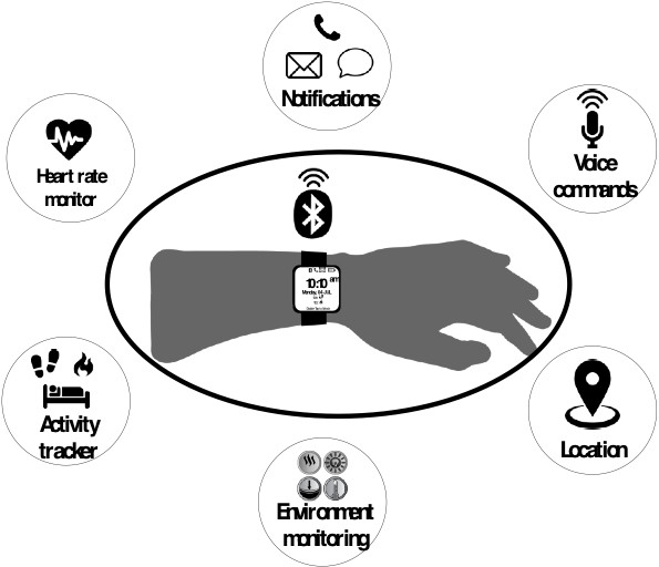
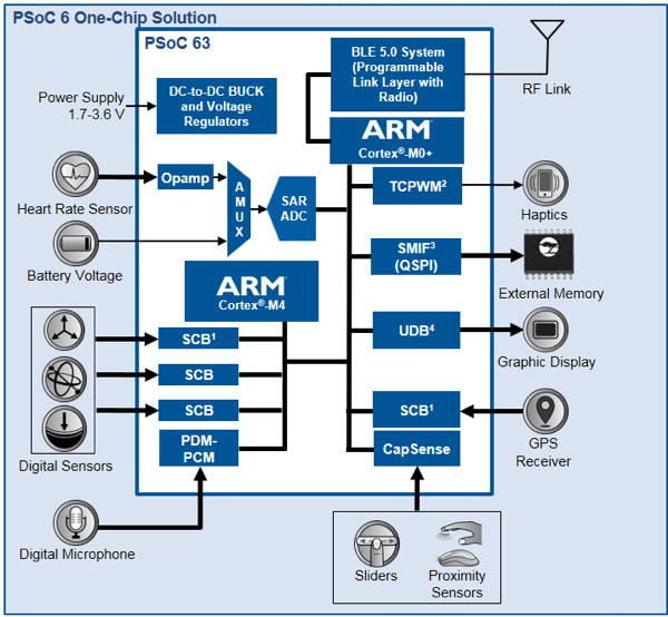
Activity Monitoring: A pedometer and calorie counter calculates the number of steps taken by a person and calculates the number of calories burned. To detect steps, an accelerometer sensor is required. A pressure sensor is also used to measure the elevation changes while walking/running. Most sensors have a digital interface, typically I2C, SPI, or UART. Additional filtering and processing is required on the acquired data to calculate values like step count, altitude, calories burned, and so on. These sensors are also used for implementing low-power system functions like waking up the complete system when motion is detected so real-time analysis can be performed. To support the multiple sensors a wearable device is likely to require, the embedded MCU will need several digital interfaces. Ideally, these interfaces can be configured between I2C, SPI, and UART to give developers the most flexibility in sensor selection and implementation. Additionally, the embedded MCU needs to support a dual core architecture with an MCU capable of performing sensor fusion and complex analysis and a low power MCU for performing system tasks like wake-on-motion.
Environment Monitoring: A monitor will may also need to collect environmental data, such as UV exposure measurements, ambient temperature, atmospheric pressure, compass heading, etc.
GPS: GPS sensors are usually digital sensors with a UART interface. GPS sensors provide positional (latitude and longitude), speed, and altitude information.
Audio: Audio signal processing in the digital domain is an essential part of any audio system before audio data is transmitted over a wireless link. Data are typically collected using a PDM microphone-based sound meter that is then measured, filtered, and/or compressed. An embedded MCU with integrated DSP capabilities and audio capabilities can greatly simplify the design of a high-quality, uninterrupted acoustic audio subsystem.
Security: Wearables need to be able to keep up to date with continuously changing security protocols and measures. An embedded MCU with secure boot capabilities ensures that the wearable device will only execute authenticated code. Additionally, devices can support Over the Air (OTA) updates to make updates transparent to users.
User interface: Today’s users have become accustomed to touch displays utilizing buttons, sliders, and proximity sensing. An embedded MCU that can also support different output types can support various display technologies such as Eink, OLED, and others.
Wireless Connectivity: Devices need to support Bluetooth Low Energy (BLE) connectivity with necessary services for wearable device operation.
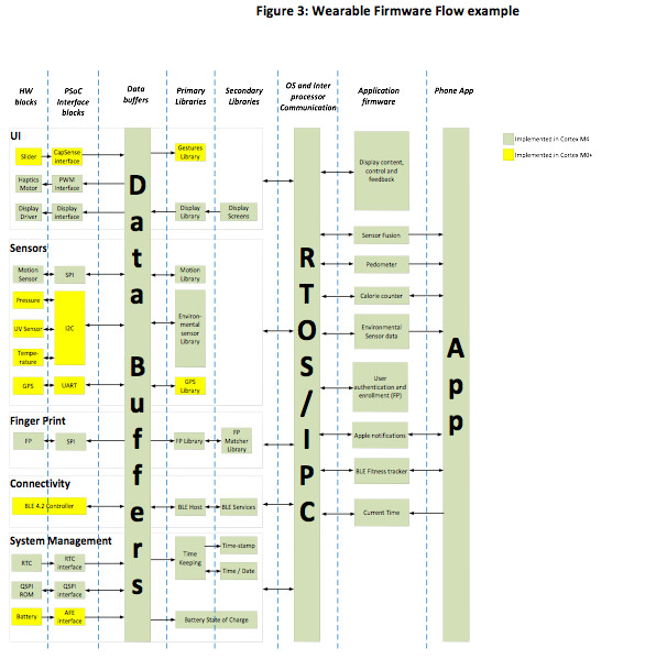
Support for all of these features requires a comprehensive firmware flow (see Figure 3). Manufacturers who support wearables applications can supply complete libraries that can accelerate development and lower overall design investment.
Task Architecture
In any wearable design, there are three key tasks:
- Acquiring data
- Processing data
- Communicate with the User – Input and Output (Display)
Typically, sensor acquisition requires a higher rate of processor operation than other tasks, given that such processing includes filters that operate on a large sample base. Thus, it is more power efficient to perform sensor data acquisition using a low power core like an Arm Cortex-M0+. Processing sensor data depends on the complexity of the algorithms used, and developers must trade off between power efficiency and processing speed. For light processing, the same low power core used to acquire sensor data can be used. For more real-time operations, however, a higher performance processor, such as an Arm Cortex M3/M4 core, is required. The user interface, usually a lightweight process when it comes to a simple wearable display and input, can be handled by either core but is ideally implemented on a low power core. Thus, to achieve the best possible performance in a wearable with low power, a dual-core architecture is needed. Note that a dual-core architecture can be leveraged to pipeline the firmware framework to improve responsiveness by speeding task completion as well as reduce resource and power consumption by sharing resources such as clocks, RAM, Flash, etc. between the cores.
The low power processor, such as Cortex M0+, runs a simple task scheduler that handles frequent, low-bandwidth tasks such as:
- Sensor data acquisition
- Capacitive sensing scan and processing
- BLE link layer controller maintaining BLE connections and advertisements
- System management including security tasks and sensors control
The high-performance processor, such as a Cortex M4, serves as an application processor running an RTOS and handling processor-intense application-level tasks such as:
- Sensor data processing (i.e., orientation calculations, altitude computations, etc.)
- Display graphics such as drawing text, images, shapes, etc.
- Complete fingerprint processing, including matching and enrollment algorithms
- BLE host layer tasks, which include all the services, profiles, and connection authentication
With shared memory and a fast inter-processor communication (IPC) channel bridging between the cores, communication latency is almost non-existent compared to having two devices communicate externally.
Low Power Core Task Architecture
On a high-level, the low power core executes two types of tasks – Level 1: Periodic tasks that are executed in every cycle and Level 2: Time-slotted tasks that are periodic but execute once in every ‘n’ number of cycles (n = period of the task/per cycle duration). A timer can be used to generate an interrupt to indicate the start of a cycle, say every 10 ms (100 Hz). Level 1 tasks execute one by one on the interrupt event. A time-slot variable can be incremented every interrupt and passed to the level 2 task manager. Depending on the slot number, the appropriate level 2 tasks are executed.
Table 1 provides an example of various tasks that can be implemented in the low power core.
Table 1. Low Power Core Tasks
|
Task |
Type |
Period (ms)/Slot (out of 50 slots) |
|
BLE Controller |
Level 1 |
10/- |
|
Capacitive Sensing Scan and Gesture detection |
Level 1 |
10/- |
|
GPS Acquire and Process |
Level 1 |
10/- |
|
Pressure/Temperature data acquire |
Level 2 |
500/1 |
|
UV data acquire |
Level 2 |
500/3 |
|
Battery data acquire |
Level 2 |
500/7 |
On completion of the data acquisition task or any event (like a gesture has been detected) that needs to be communicated to other tasks running on high-performance core, a message packet is formed and sent over IPC to the high-performance core. An interrupt is raised on the high-performance core, the message packet is processed, and data is appropriately passed to the intended tasks executing on the high-performance core.
High-Performance Core Task Architecture
The high-performance core uses an RTOS to manage tasks such as BLE, motion sensing, display update, GPS, pressure/temperature, UV, and fingerprint detection. Except for BLE, motion sensing, and fingerprint detection, other tasks wait for data from the low power core.
The BLE task can run periodically (once every connection interval). After completion, the task suspends itself until the next required wakeup.
The motion sensing task can be an aperiodic task that runs whenever an interrupt is raised by the motion sensor itself. Motion sensors like the Invensense MPU9255 includes a Digital Motion Processor (DMP) that collects data on an on-chip FIFO and interrupts the high-performance core at a pre-configured rate. On interrupt, the motion sensor task reads the FIFO in the motion sensor through an SPI interface and processes the data to calculate orientation, steps, calories burned, etc.
The fingerprint detection task can be an aperiodic task that runs whenever a user is enrolling, authenticating, or deleting a fingerprint. This task also runs when a user fingerprint is enrolled and the display is locked. An enrolled user fingerprint can be used to unlock and secure the wearable device.
The display task can be an aperiodic task as well that runs whenever data need to be updated on the screen (i.e., sensor data, time, battery, and BLE notifications from other tasks) or if a capacitive sensing gesture event is reported from the low power core.
The GPS, pressure/temperature, and UV tasks can be pseudo-periodic tasks because they do not suspend and wakeup periodically. Rather, task wakeup is triggered from the low power core after it collects data from the respective sensors. Since the data collection rate is periodic in the low power core, these tasks can execute in a periodic fashion on the high performance core.
Table 2 shows an example of the tasks a high-performance core manages.
Table 2. High-Performance Core Tasks
|
Task |
Priority |
Stack |
Type |
Wakeup source |
|
BLE |
9 |
500 |
Periodic |
OS wake up every BLE Connection interval (vTaskdelay) |
|
Motion Sensor |
8 |
500 |
Aperiodic |
Interrupt from sensor |
|
Display |
6 |
500 |
Aperiodic |
Notifications from other tasks |
|
Pressure |
8 |
200 |
Pseudo periodic |
Notification from low power core |
|
UV |
8 |
150 |
Pseudo periodic |
Notification from low power core |
|
GPS |
8 |
100 |
Pseudo periodic |
Notification from low power core |
|
Finger print |
7 |
5000 |
Aperiodic |
Notification from display task and interrupts (SMIF/SPI) |
Inter-Processor Communication architecture
Two cores operating simultaneously need a mechanism to protect shared data and communication for synchronizing tasks in firmware. Dual-core architectures need to support multiple IPC mechanisms such as IPC lock, message passing, and interrupt/notify. Task code can use the IPC lock feature to protect shared data and IPC message passing to exchange notifications and data between the cores.
IPC lock: Whenever shared data is accessed for modification, the accessing core/task tries to acquire a lock corresponding to the data. If the lock is free, the core/task is granted access to the data. Once the update/processing is complete, the task can release the lock to grant access of the data to other pending tasks. This protects the data from getting corrupted by multiple sources trying to update/use the data at the same time.
IPC messages: In addition to protecting shared data, a means of communication is required to synchronize tasks between the cores. This can be achieved using a “Command and parameter” message packet passing between the cores. Whenever a core wants the other to perform an action, it packs the action/command ID with any required parameters into a message and passes the message over the IPC. Once the message packet is ready, the core triggers an IPC interrupt on the other core, where the command is parsed and then acted upon.
In part II, we discussed wearables applications with an example implementation. In part III, we will illustrate how a wearable implementation can be leveraged to interact with a smart home network.
References:
- PSoC® 6 MCU: PSoC 63 with BLE Datasheet Programmable System-on-Chip (PSoC®)
- PSoC 63 with BLE Architecture Technical Reference Manual (TRM)
- AN210781 - Getting Started with PSoC 6 MCU with Bluetooth Low Energy (BLE) Connectivity
- AN219528 - PSoC(R) 6 MCU Low-Power Modes and Power Reduction Techniques
- AN215656 – PSoC 6 MCU Dual-Core CPU System Design
- AN213924 - PSoC 6 MCU Bootloader Software Development Kit (SDK) Guide
- AN217666 – PSoC 6 MCU Interrupts
- AN218241 - PSoC 6 MCU Hardware Design Considerations
- AN92239 - Proximity Sensing with CapSense®
- AN219434 - Importing PSoC Creator Code into an IDE for a PSoC 6 Project
- AN91445 - Antenna Design and RF Layout Guidelines
Authors:
Jaya Kathuria works as an Applications Manager at Cypress Semiconductor Corporation where she is managing the Embedded Applications Group and Solutions Development using the PSoC platform. She has 13+ years of experience in Semiconductor Industry. She earned an executive management credential from IIM, Bangalore and holds a BS in Electronics Engineering from the Kurukshetra University. Jaya can be reached at [email protected].
Meenakshi Sundaram is a Senior Staff Applications Engineer at Cypress Semiconductor Corporation. He works on Bluetooth low energy and System-on-Chip solution development with Cypress’ PSoC platform. He has 7+ years’ experience in Embedded System and Solution development. He holds a MS degree in Embedded Systems from the Birla Institute of Technology, Pilani. He can be reached at [email protected].


