
Microfluidics: Key Concepts and Applications - Part 2
June 14, 2019
Story

Microfluidics is a multidisciplinary field in which collaboration between chemists, physicists, biotechnologists, doctors and different engineering disciplines is needed.
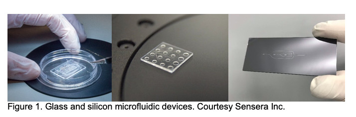
Fabrication of Silicon and Glass Devices
The glass and silicon microfluidic chips are fabricated by adapting some well-known microelectromechanical systems (MEMS) and semiconductors techniques. Processes such as photo or e-beam lithography, thin film deposition, wet and dry etch, wafer bonding, and laser machining are commonly used to manufacture microfluidic devices in microfab foundries like Sensera, Inc.
The starting materials are silicon or glass wafers, usually with a 675 µm thickness, and 150 mm in diameter. Wafers are also available in 100, 200, 300 and even 450 mm diameter and different thicknesses.
Prior to starting any processes on substrates, typical contaminants must be removed (step 1 in schematic): dust from scribing or cleaving (minimized by our laser scribing), environment particles (minimized by our good clean room practices and a tight SPC control on particles’ count), any photoresist residues from previous photolithography (minimized by performing oxygen plasma ashing), bacteria (minimized by good DI water system) or any solvent, water or organic residues.
Then, to define the desired design or pattern on the cleaned substrate we use a lithography process, which is basically the transfer of geometric shapes from a photomask to the selected substrate. The process itself goes back to 1796 when it was a printing method using ink, metal plates and paper. Nowadays, the photolithography uses optical radiation to image the mask or design onto glass or silicon wafer using photoresist layers.
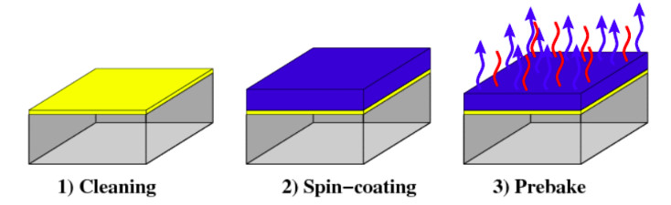
The wafers are spin coated with a thin layer of photoresist (2), i.e. light sensitive polymer, after applying an adhesion promoter layer. Thickness of the layer varies depending on viscosity of photoresist chosen and spin speed (typically between 1000 to 4000 RPM for 30-70 seconds). Thicknesses from 1 to 60 µm can be obtained in this process and will be selected based on the minimum features size that needs to be resolved. The photoresist layer is prebaked (3) to evaporate the coating solvent and to densify the resist after spin-coating. Baking the resist in a hot plate is usually faster, more controllable, and does not trap solvent like convection oven baking. The thickness of the resist is usually decreased by 25 percent during prebake for both positive and negative resists. Decreasing the prebake increases the development rate.
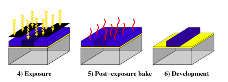
The coated substrate is exposed to UV light (4), in a mask aligner, through a photomask containing the desired pattern. For simple contact, proximity, and projection systems, the photomask is the same size and scale as the printed wafer pattern – i.e. the reproduction ratio is 1:1. Steppers are projection systems that give the ability to change the reproduction ratio, which allows larger size patterns on the mask. This process is more robust to mask defects and alignment is more precise. We have both options, mask aligner and stepper, at Sensera. Depending on photoresist chosen, i.e. negative or positive, the exposed photoresist is crosslinked, or dissolved in a developer bath. A post-exposure bake (5) helps improve the definition of the pattern.
After development (6) of the unexposed or exposed areas, the resulting pattern defined in resist on the wafer acts as a mask for etching. Postbake or hardbake (7) removes any remaining traces of the coating solvent or developer. This eliminates the solvent burst effects in subsequent vacuum processing but introduces some stress, and sometimes even shrinkage, into the photoresist. In addition, longer or hotter postbake makes resist removal much more difficult. This step must be controlled and only added as required.
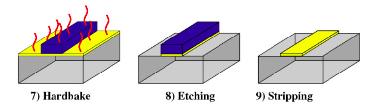
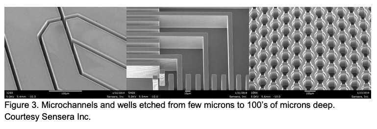
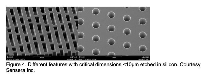
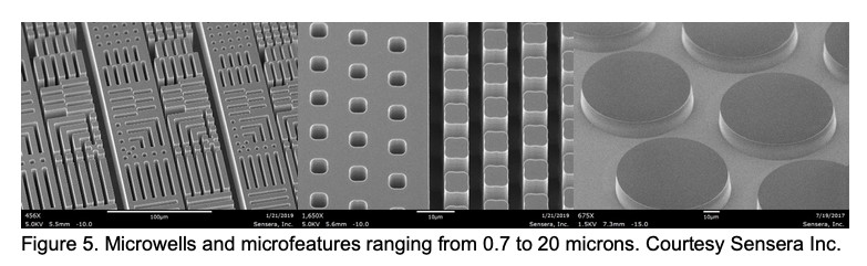
Wet or dry etch (8) is performed to transfer the pattern from the mask to the silicon or glass substrates by etching (or removing) the material that is unprotected by the mask. This is an irreversible process that will create the 2D replica of the designed pattern on the substrate. Depth of features is controlled by etching time as desired and always measured. When deep features are desired, more selective masks such as metals or silicon dioxide should be used.
After etching, the mask is removed (9). Simple solvents are generally enough to remove non-postbaked photoresists while plasma etching with O2 (ashing) is better at removing any remaining polymer debris. Channels can be closed by bonding the etched substrate to another substrate. Different bonding processes can be used depending on factors such as the material to be bonded to (i.e. glass, silicon or polymer), temperature requirements, etc.
Processes can vary greatly for different specific designs. Multiple photolithography and etching steps, or bonding processes can be done in the substrates to obtain multiple depths and layers. Processes parameters can also be tuned to change some device properties, such as surface roughness, hydrophobicity or optical transparency in certain wavelength bands. Higher surface roughness, for example, could be beneficial when higher surface area is needed in the devices. However, that same parameter could be detrimental for specific applications in which cells could be damaged by the roughness.
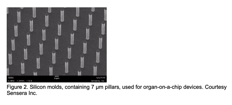
In recent developments at Sensera, etching depths of up to 800 µm have been produced for serpentine microchannels. Features with critical dimensions as low as 1 um can be produced with aspect ratios as high as 1:30. As an example, Sensera currently fabricates micropillar molds for organ-on-a-chip devices that have very challenging dimensional and defect tolerances, i.e. 7 ± 0.7 µm diameter with a 50 ± 7 µm height, and no defects larger than 30 µm anywhere in the etched area, and no more than 5 defects smaller than 30 um within a 1 mm² section of the etched area, respectively. These are very tight tolerances considering the large size of the die – i.e. 45 mm². Implementing a very stringent quality system and precisely controlling the photo CD and the etch uniformity has led us to continuous delivery of these products (De Jesus, 2018).
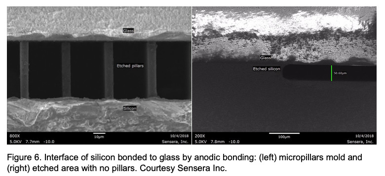
In addition, Sensera has demonstrated high expertise in anodic bonding of silicon to glass, silicon to polymer bonding, and fusion bonding of identical materials, etc., enabling new cell biology innovations.
Microfluidics Applications
Organs-on-chip devices
Organs-on-chip are microfluidic cell culture devices that provide an in vitro experimental platform to emulate organs by modeling their functions, without the need to conduct experiments on humans or animals. They are used to fast-track drug development, aiming to reduce animal testing, and for the implementation of personalized safety testing of new drugs.
They can enable accurate monitoring of drug efficiency. These devices can also be applied to disease modeling and precision personal medicine. Heart, lung, kidney, liver, brain, and skin are organs that have already been reproduced using microfluidic devices, either by themselves (single organ-on-a-chip) or combined with one or more other organs (multi organ-on-a-chip) (Ronaldson-Bouchard and Vunjak-Novakovic, 2018).
Point-of-care and lab-on-a-chip devices
These devices use microchannels that are coupled with chambers or wells filled with reagents to detect and measure specific biomarkers for diagnostic purposes. They can also be used for rapid and sensitive investigation of nucleic acid samples, DNA and RNA, and proteins. An electric field created in these devices causes proteins, DNA and RNA to migrate along a separation channel to be subsequently measured by a detector.
Cell culture devices
These are used in cell biology studies. They promote the understanding of physiological and pathological changes in cells, such as cancer cells and stem cells, in a controlled environment. They have the potential to improve the physiological relevance of in vitro models in the study of cancer (TMR, 2018).
Droplet microfluidic devices
These are devices in which channel geometries and/or electrostatic forces interact with liquid to create or manipulate droplets. Droplets can then have specific characteristics that allow localized reactions, while preventing diffusion of compounds outside the droplet.
# # #
About Sensera
Sensera Inc. (MicroDevices) is an ISO 9001 registered designer and manufacturer, and ISO 13485 registered manufacturer of specialized high-performance sensors and modules. Sensera's core expertise in MEMS based technologies is bringing custom devices from concept to market. Sensera provides guidance to their customers through specific phase-gate stages of design and materials selection, development, validation and into production. Collaboratively working with the customers, they ensure the combined efforts enable an efficient use of resources from concept to the production quality devices.
Sensera combines internal facilities with a rapidly reconfigurable external network to deliver cost effective devices with the highest quality, on-par with mega-volume suppliers, but with a faster turnaround for far lower minimum volume requirements.
Marisel De Jesús Vega, Program Manager at Sensera Inc., received her B.S. from University of Puerto Rico, Mayagüez campus and her Doctoral degree from University of Massachusetts Lowell, both in Chemical Engineering. Her interests are microfluidic devices, microfabrication and materials.
References
- M. De Jesus Vega, "Manufacturing MEMS to the quality standards of multiple industries," Embedded Computing Design, June 21, 2018.
- G.S. Fiorini and D.T. Chiu, "Disposable microfluidic devices: fabrication, function, and application," BioTechniques, vol. 38. No. 3, pp. 429-446, 2005.
- R. Novak, M. Didier, E. Calamari, C.F. Ng, Y. Choe, S.L. Clauson, B.A. Nestor, J. Puerta, R. Fleming, S.J. Firoozinezhad, and D.E. Ingber, "Scalable Fabrication of Stretchable, Dual Channel, Microfluidic Organ Chips," Journal of Visualized Experiments, 140, 2018.
- K. Ren, J. Zhou and H. Wu, "Materials for Microfluidic Chip Fabrication," Accounts of Chemical Research, vol. 46, no. 11, pp. 2396-2406, 2013.
- K. Ronaldson-Bouchard and G. Vunjak-Novakovic, "Organs-on-a-chip: A Fast Track for Engineered Human Tissue in Drug Development," Cell Stem Cell Review, 22, 2018.


