
Lattice Unveils Low-Power FPGA Platform, Updates Lattice Radiant Design Software
December 12, 2019
Product

The platform addresses a range of applications, including AI for IoT, video, hardware security, embedded vision, 5G infrastructure and industrial/automotive automation.
The creation of advanced electronic devices has become simultaneously more easy and difficult; there are more and more solutions out there, enough to address almost every application. The biggest problems we face include technology integration and cost-effective commercialization.
This has given rise to the creation of integrated, scalable, device solutions, where a modular, building-block approach is available using stackable functionalities in a single application solution. This scalable approach is often supported by advanced software suites that streamline and simplify the design effort. One such solution set was recently announced by Lattice Semiconductor in their new low power FPGA platform, Lattice Nexus.
Touting its energy-efficient performance, the platform addresses a range of applications, including AI for IoT, video, hardware security, embedded vision, 5G infrastructure and industrial/automotive automation. The Lattice Nexus platform provides system-level solutions that combine design software and pre-engineered soft IP blocks with evaluation boards, kits, and reference designs, with solutions like sensor bridging, sensor aggregation, and image processing.
Features include optimized DSP blocks, and higher on-chip memory capacity for power-efficient computing, such as AI inferencing algorithms, and can run twice as fast at half the power of Legacy FPGAs. Additional features include programmable power/performance optimization and fast configuration for instant-on-type applications. Lattice Nexus is developed on high-volume 28 nm fully-depleted silicon-on-insulator (FD-SOI) process technology from Samsung, with 50 percent lower transistor leakage compared to bulk CMOS.
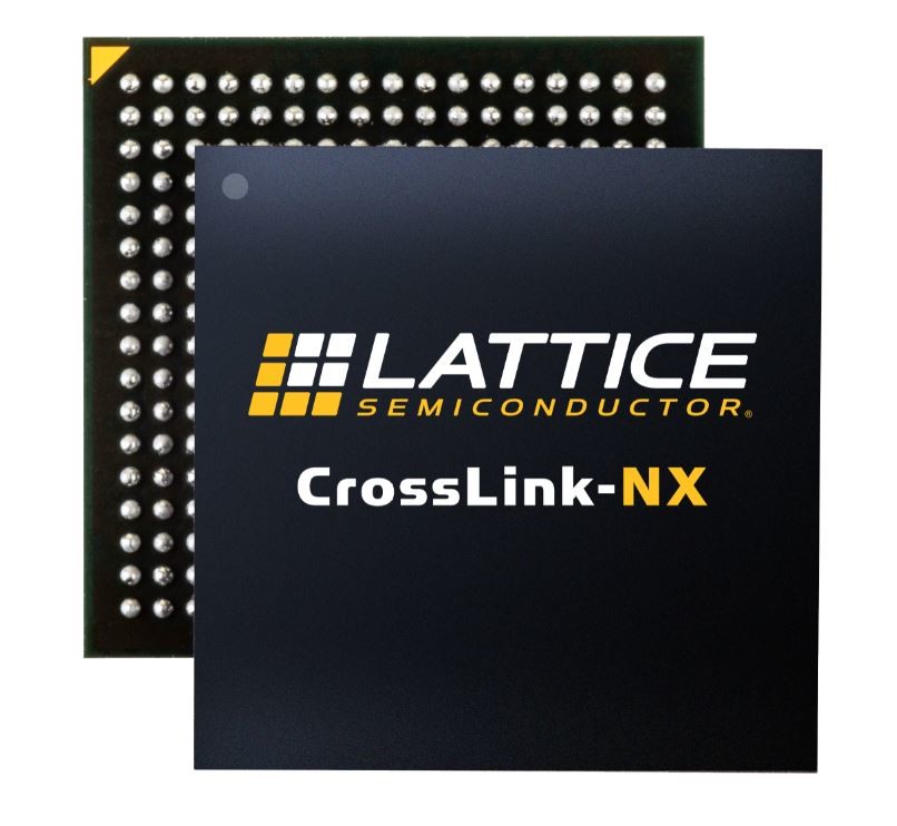
In another major move, the company also released the latest version of its software design tool for FPGAs, Lattice Radiant 2.0. In addition to adding support for higher density devices like the CrossLink-NX FPGA family, the updated design tool also offers new features that make it faster and easier than ever to develop Lattice FPGA-based designs.
The design software leads designers through the design flow from design creation, to importing IP, to implementation, to bitstream generation, to downloading the bitstream onto an FPGA. An on-chip debugging tool allows users to conduct bug fixes in real time, and lets a developer insert virtual switches or LEDs in their code to confirm viability. The tool also lets users change hard IP block settings to test different operating modes.
Improved timing analysis provides more accurate trace and route planning and clock timing to avoid design congestion and thermal issues, and an engineering change order (ECO) editor lets developers make incremental changes to a completed design without having to recompile the entire FPGA database. Also, a Simultaneous Switching Output (SSO) calculator analyzes the signal integrity of individual pins to ensure their performance isn’t adversely affected by their proximity to another pin.


