
Simplifying AI Edge Compute at < 2mW
November 26, 2018
Blog

The Tensai architecture employs multiple voltage regulators to support ultra-low-power, always-on processing at less than 2 mW for coin cell or solar cell-powered AI systems.
As IoT developers solve the connectivity, manageability, and security challenges of deploying devices at the edge, requirements now turn to making these systems smarter. Engineers are now tasked with integrating artificial intelligence (AI) into embedded systems at the far reaches of networks, which must minimize power consumption, communications latency, and cost while also becoming smarter.
Unfortunately, many of the processing solutions available for embedded AI are too power hungry, too difficult to program, or too expensive for edge applications.
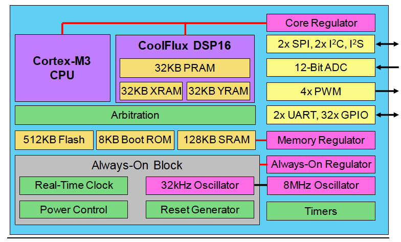
To thread the needle between higher performance, power consumption, cost, and ease of use, fabless SoC vendor Eta Compute’s Tensai chip combines an asynchronous Arm Cortex-M3 CPU, NXP CoolFlux DSP16 core, and low-power analog blocks in a 55 nm ULP process (Figure 1). The Tensai solution also incorporates a neural network software stack for implementing convolutional neural networks (CNNs) and spiking neural networks (SNNs) that execute locally on the DSP’s dual 16x16 MACs.
Edge AI at < 2mW
The Tensai architecture employs multiple voltage regulators to support ultra-low-power, always-on processing at less than 2 mW for coin cell or solar cell-powered AI systems. These include a dedicated regulator for the chip’s real-time clock and reset circuits, another reserved for memory blocks, and a third for the MCU and DSP cores.
The device consumes only 600 nanoamps with just the always-on block powered on. That number increases to 10 microamps in sleep mode with the memory blocks powered.
However, Tensai’s ultra-low-power profile does not limit the SoC in AI workloads. The CoolFlux DSP16 core operates at up to 100 MHz, which provides 200 million 16-bit MACs per second of performance. Performing inference on 32x32-pixel images from the CIFAR-10 data set, Tensai can process five images per second at 0.4 millijoules per image.
For non-DSP engineers, Tensai’s neural network software stack abstracts hardware programming complexity by allowing developers to pass quantized TensorFlow Lite models through an interpreter on the Cortex-M3. The Cortex-M3 then generates code that are translated into functions that can be carried out on the DSP.
A four-channel DMA engine transfers data between I/Os and 32 KB PRAM and 64 KB of joint XRAM and YRAM reserved for the DSP. The CoolFlux core can also handle two 8x8 MACs in addition to 16-bit resolutions.
On the edge of AI
The ultra-low power consumption and ease of programming will help bring AI to general embedded and IoT engineers as they add intelligence to the edge. Other high-level features of the Tensai chip that will be familiar to embedded and IoT developers include:
- 512 KB flash (enough for about 450,000 neural network weights)
- 128 KB SRAM shared between the Cortex-M3 and DSP
- 4x ADC channels (12-bit ADC consumes uW at 200,000 samples/s)
- 4x PWM channels
- I2S, I2C, SPI, UARTs, GPIOs
Initially, Tensai will be manufactured in a 10 mm QFN-88 package, with volume pricing estimated at $5.00. First shipments are expected in 1Q19.
For more on Eta Compute’s edge AI solutions, visit etacompute.com.


