
X-FAB Brings 180nm Automotive-Qualified Semiconductor Process to its French Site
August 02, 2019
News

X-FAB Silicon Foundries announced that its high-voltage 180nm CMOS semiconductor process is now available for automotive applications via the company?s production facility in France.
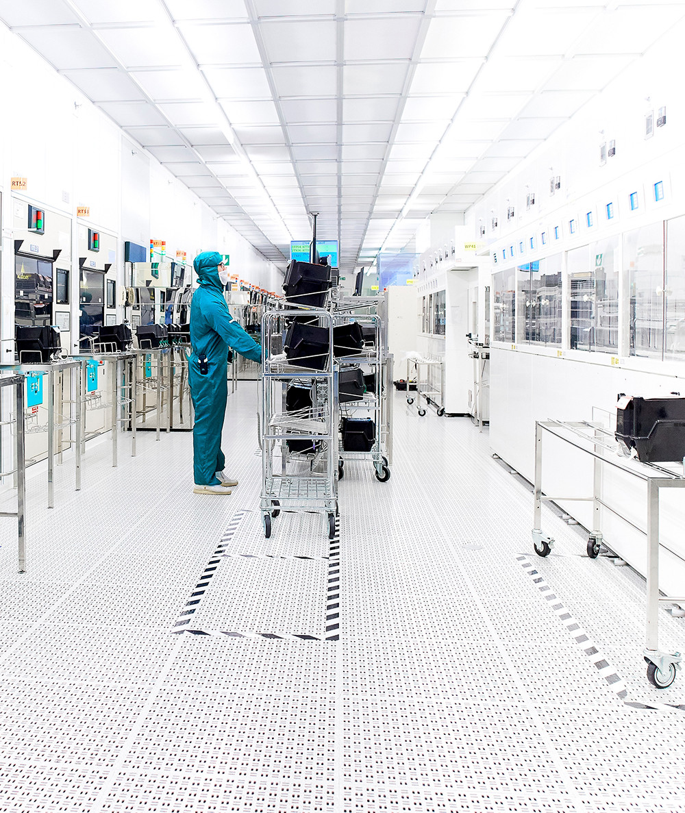
X-FAB Silicon Foundries announced that its high-voltage 180nm CMOS semiconductor process is now available for automotive applications via the company’s production facility in France. Located in Corbeil-Essonnes, the X-FAB manufacturing plant is the company’s largest in Europe, with 15,000m² of used cleanroom area, with additional 9,000m² cleanroom space that can be equipped for future demand.
Specifically optimized for automotive, industrial and medical applications, the XH018 mixed-signal process has a modular architecture. Besides supporting high-temperature and low-leakage operation, XH018 comes with advanced PDK features to improve design robustness. The offering includes advanced digital memory IP as well as analog/mixed-signal reference design kits and tools for checking operating conditions and ESD robustness.
“We are very pleased that our XH018 high-voltage process, currently running in our high volume fab in Malaysia, has now been successfully installed also in France. With this, we now have a dual source for our main 180nm platform and the capacity needed to serve the increasing demands of our customers,” stated Rudi De Winter, X-FAB’s CEO.
For more information, visit www.xfab.com.


