
TIA Fundamentals: The Parasitics Part 3
January 20, 2020
Story
The DC transimpedance amplifier discussion, in my previous blog: TIA Fundamentals Part 2: Signal Frequency Response, is a good start towards understanding the AC signal response.
The DC transimpedance amplifier discussion, in my previous blog: TIA Fundamentals Part 2: Signal Frequency Response, is a good start towards understanding the AC signal response. But that is not all. You probably want the signal going through your transimpedance amplifier circuit (TIA) to be stable.
Back to our standard TIA circuit (Figure 1).

Figure 1. Standard high-precision TIA circuit without parasitic capacitances.
I know that this is a light-to-current converter, but now that we have an amplifier that outputs a voltage signal, the determination of the circuit’s stability resides in the voltage domain. The circuit in Figure 1 has the potential to be unstable, but with your newly learned design expertise in this blog, you will be on your way to understanding the players in the TIA game. The keys to TIA stability lie within the amplifier and feedback component parasitics.
Amplifier and Feedback Circuit’s Parasitics
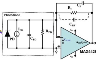
Starting with the amplifier circuit, there are four additional parasitic capacitances hidden in this circuit; CRF, CCM+, CCM-, and CDIFF (Figure 2).

Figure 2. This diagram explicitly draws out the parasitic capacitances of the amplifier circuit.
The parasitic amplifier capacitances are CCM+, CCM-, and CDIFF. CCM+ and CCM- are the input common-mode amplifier capacitances. You will notice that CCM+ is biased from a ground connection to a virtual ground in the amplifier. Hence, we will ignore CCM+ and call CCM-, simply CCM. CDIFF is definitely in the circuit, and it is actually in parallel with CCM. This fact conveniently makes the amplifier’s input capacitance equal to CCM + CDIFF, which we will call CAMP.
In the top of Figure 2, there is a parasitic capacitance (CRF) across the feedback resistor, RF. This capacitance is a consequence of the parasitic capacitance across the discrete resistor plus PCB parasitic parallel capacitances in the layout. Typically, the cumulative value of all these parasitic capacitances is at the most a few picofarads. If the PCB designer is aware of this problem, a careful layout can reduce this capacitance to below 1pF. You may think that this small capacitance is negligible until we calculate the feedback capacitor (CF) value but let’s put off this final decision until the end of our design work. The amplifier in Figure 2 has three parasitic capacitances, CCM-, CDIFF, and CCM+.
The definitions or the component labels in Figure 2 are:
CF = TIA feedback capacitor.
RF = TIA feedback resistor.
CRF = TIA feedback resistor parasitic capacitance.
CCM-, CCM+ = Common-mode amplifier capacitance.
CDIFF = Differential amplifier capacitance.
AOL(jw) = Amplifier open-loop gain.
Modified variables:
CCM- = CCM
CAMP = CCM + CDIFF
It is useful to note that CAMP is in parallel with the photodiode (PD). Put quite simply, if the photodiode has any parasitic capacitance, the amplifier’s capacitances add to the photodiode’s capacitance. We will learn about how this impacts the circuit stability later.
Photodiode Parasitics
The photodiode receives the light signal. In this circuit, the incident light on the photodiode causes current (IPD) to flow through the diode from cathode to anode. The amplifier’s inverting input impedance is extremely high, making the current generated by the photodiode flow through the feedback resistor, RF (Figure 3).

Figure 3. Photodiode parasitics include the junction capacitance (CPD) and junction resistance (RPD).
In Figure 3, the definitions of the parasitic components are:
PD = Ideal photodiode.
IPD = Current generated by illuminating light on the photodiode.
CPD = Photodiode parasitic capacitance.
RPD = Photodiode parasitic parallel resistance.
When light impinges on the photodiode, the current (IPD) conducts from the cathode of the diode to the anode. For example, with RF and CF equaling 1MW and 2.5pF, inclusive, and IPD equaling a DC (1mA), the signal transfer function’s pole equals 1/(2p RF x CF) or 63.7kHz and the amplifier output voltage, VOUT, equals IPD x RF or +1V. A reduction in RF moves this pole to a higher frequency value and output voltage to a lower voltage.
The total picture of this transimpedance amplifier includes all components along with their parasitic capacitors and resistors (Figure 4).

Figure 4. Complete circuit diagram of the transimpedance amplifier including parasitic capacitors and resistors.
In Figure 4, the amplifier’s input bias currents must be lower than the minimum photodiode current. It is a rule of thumb to use FET or CMOS input amplifiers with input bias current specifications less than 10pA, such as the MAX44260, with a typical input bias current specification equaling 0.01pA.
The offset voltage error of a particular amplifier may or may not be a problem depending on the application circuit. An amplifier with a high offset voltage (10s of millivolt range) can dramatically compromise the circuit’s linearity and dynamic range.
In precision applications, the amplifier’s offset voltage across the photodiode impacts the circuit’s low-light input linearity by generating a current that is not associated with the light hitting the photodiode.
The offset voltage may also impact the TIA’s dynamic range. For example, the circuit design in Figure 1has a voltage gain of (1 + RF / RPD). The offset voltage times this gain factor transmits to the amplifier’s output. In this example, RF equaling 1MW and RPD equaling 1GW, is equal to 1.001V/V. An amplifier with an offset voltage of 10mV would have a constant DC error at the output of 10.01mV. In a 5V system, 10.01mV lessens the dynamic range by approximately 0.2%. In Figure 4, the maximum MAX44260 input-offset voltage equals 50mV, rendering a 0.001% dynamic range error.
I will tease you with the TIA bode plot (Figure 5) with little or no explanation for now. In this plot, you will see these parasitic components pop out, which will send us on our way to the stable TIA circuit. See you in the next blog that will dig into the details of this bode plot.

Figure 5. The closure rate between the closed-loop gain (1/β) and the amplifier’s open-loop gain (AOL) is 20dB/decade, which determines circuit stability.


