
Programmable Gain Instrumentation Amplifiers: Finding One that Works for You
September 24, 2020
Blog
Data acquisition (DAQ) systems find their use in many industries, for a wide range of applications, such as research, analysis, design verification, manufacturing, and testing.
Data acquisition (DAQ) systems find their use in many industries, for a wide range of applications, such as research, analysis, design verification, manufacturing, and testing. By nature, these systems interface to various sensors, which poses a challenge to the front end. Different sensor sensitivities must be considered—for example, a system may need to interface to a load sensor that has a maximum output of 10 mV and submicrovolt sensitivity, while also interfacing to a sensor that is preconditioned for a 10 V output. With a single gain, the system needs to have a very high resolution to sense both inputs. Even then, signal-to-noise ratio (SNR) is sacrificed at the lowest inputs.
In these applications, programmable gain instrumentation amplifiers (PGIAs) are a good solution for the front end to accommodate the sensitivities of the various sensor interfaces, while optimizing SNR. Integrated PGIAs are available to achieve good dc and ac specifications. This article discusses the various integrated PGIAs and the advantages in using them. Limitations will also be discussed, along with guidelines for building a discrete PGIA when trying to meet a specific requirement.
Integrated PGIAs
ADI offers a number of integrated PGIAs in its portfolio. Integrated PGIAs provide the benefit of shorter design time and a smaller footprint. The digitally adjustable gain is achieved with internal precision resistor arrays. On-chip trimming of these resistor arrays can be done to optimize gain, CMRR, and offsets, resulting in good overall dc performance. Design techniques can also be utilized for compact IC layout to minimize parasitics, as well as provide excellent matching, resulting in good ac performance. Because of these advantages, it is always recommended to choose an integrated PGIA, if there is one that meets the design requirement. Table 1 lists available integrated PGIAs along with some key specifications.
Table 1. Programmable Gain Instrumentation Amplifiers Specifications

The choice of PGIA is dependent on the application. The AD825x is very useful in multiplexed systems due to its fast settling time and high slew rate. The AD8231 and LTC6915, which have zero-drift architectures, are useful for systems where precision performance is required over a wide range of temperatures.
There are also a number of component solutions that integrate the multiplexer, PGIA, and ADC to form a complete DAQ solution. Examples of these are the ADAS3022, ADAS3023, and the AD7124-8.
Table 2. DAQ System Specifications

The choice of these solutions will mainly depend on the specifications of the input signal sources. The AD7124-8 is designed for slower applications that require very high precision, such as temperature and pressure measurements. The ADAS3022 and ADAS3023 are useful in relatively higher bandwidth applications such as in process control or power line monitoring. They do, however, consume more power in comparison to the AD7124-8.
Implementing a Discrete PGIA
Some systems may need to meet one or two specifications that are not achievable with the aforementioned integrated devices. Typically, the following requirements would necessitate the user to instead build their own PGIA using discrete components:
- Very high scan rates in multiplexed systems that require higher bandwidth
- Ultra-low power
- Customized gains or attenuation in the system
- Low input bias current for high impedance sensors
- Very low noise
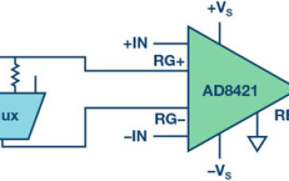
One of the approaches commonly used in designing discrete PGIAs is to use an instrumentation amplifier with the desired input characteristics, for example, the low noise of the AD8421, accompanied with a multiplexer to switch in the gain resistor to vary the gains.

(Figure 1. AD8421 with mux for switched-in gain.)
In this configuration, the on-resistance of the mux is effectively in series with the gain resistor. A problem arises as this on-resistance changes with respect to the voltage present at the drain. Figure 2, taken from the ADG1208 data sheet, demonstrates this relationship.

(Figure 2. On-resistance vs. drain voltage for ADG1208.)
The series combination of the on-resistance and the gain resistor results in a nonlinearity in the gain. This implies that the gain will change along with the common-mode voltage, which is not desirable. For example, the AD8421 requires a gain resistor of 1.1 kΩ for a gain of 10. For the ADG1208, the on-resistance changes by as much as 40 Ω with the source or drain voltage varying from ±15 V. This results in a gain nonlinearity of about 3%. For larger gains, this error will become even more apparent, and the on-resistance may even start to become comparable to the gain resistor.
Alternatively, one could use multiplexers with low on-resistance to minimize this effect, but this comes at the price of higher input capacitance. Table 3 demonstrates this with a comparison of ADG1208 and ADG1408.
Table 3. On-Resistance vs. Capacitance Trade-Off in Multiplexers

The input capacitance of the switch leads to another problem in the configuration in Figure 1, because the RG pins on any given three pin op amp in-amp are very sensitive to capacitances. The capacitances of the switch could cause peaking or instability in this circuit. A bigger problem is that the capacitive imbalance on the RG pins leads to a reduction of ac common-mode rejection ratio (CMRR), which is a key specification of instrumentation amplifiers. The simulation plot in Figure 3 shows how CMRR degrades with different multiplexers across the gain pins of the AD8421. The plot clearly shows that with increasing capacitance, there is more degradation in CMRR.

(Figure 3. Simulated CMRR with different switches.)
In order to alleviate the ac CMRR degradation, the best solution is to ensure that the RG pins see the same impedance. This can be done by balancing the resistors and placing the switching component in between the two resistors, as shown in Figure 4. A multiplexer does not work in this case due to the inherent capacitive imbalance on the two ends of the switches. Also, because the drains of the multiplexer are shorted together, only a single resistor can be used on one side of the RG pins, which still leads to imbalances.

(Figure 4. Discrete PGIA using a balanced configuration.)
A quad SPST switch such as the ADG5412F is recommended in this case. Apart from the fact that the switch gives the flexibility to use balanced resistors, the capacitances are also balanced for the drain and source, which reduces the degradation on CMRR. Figure 5 shows the comparison of the ac CMRR when a multiplexer is used across the gain pins of the AD8421 vs. when a quad SPST switch is used.

(Figure 5. CMRR simulation with an SPST switch vs. mux configurations.)
The ADG5412F also has low on-resistance, which is very flat across drain or source voltage, as shown in Figure 6. It is specified to change to a maximum of 1.1 Ω over the drain or source voltage. Going back to the initial example, with the AD8421 in a gain of 10 and a gain resistor of 1.1 kΩ, the switch would introduce only 0.1% of gain nonlinearity. There is still a component of drift though, which will be more pronounced at higher gains.

(Figure 6. On-resistance of ADG5412F over common-mode voltage.)
In order to eliminate the parasitic resistance effects of the switch, an in-amp with a different architecture can be used to implement arbitrary gains. The AD8420 and AD8237 have an indirect current feedback (ICF) architecture, and are good choices for applications that require low power and low bandwidth. In this configuration, the switch is placed in a high impedance sense path, so the gain is not affected by the changing on-resistance of the switch.

(Figure 7. Discrete PGIA using in-amps with indirect current feedback.)
For these amplifiers, the gain is set with the ratio of the external resistors in the same way as a non-inverting amplifier. This gives the user more flexibility as the gain-setting resistors can be chosen depending on the design requirement. Standard thin film or metal film resistors can have temperature coefficients as low as 15 ppm/°C. This gives better gain drift than standard instrumentation amplifiers that set the gain with a single external resistor, where mismatch between the on-chip and external resistors typically limit the gain drift to around 50 ppm/°C. For the best gain error and drift performance, a resistor network can be used for its tolerance and temperature coefficient tracking. This does come at the expense of cost, though, so unless it is needed, discrete resistors are preferred.
Another solution, and the one that provides the most flexibility, is the three op amp in-amp architecture with discrete components, as shown in Figure 8, with multiplexers to switch in gain resistors. There is a much larger variety of operational amplifiers to choose from compared to instrumentation amplifiers, so designers have more choices, which allows them to design around a specific design requirement. Special functions such as filtering can also be built into this first stage. A difference amplifier in the second stage completes this architecture.

(Figure 8. Discrete PGIA.)
The choice of the input amplifiers is directly dependent on the DAQ requirement. For example, a low power design will require the use of amplifiers with low quiescent current, while systems that expect to see high impedance sensors at the input might make use of amplifiers with very low bias current to minimize error. Dual amplifiers should be used for better tracking over temperature.
It can be noted that, when using the configuration in Figure 8, the on-resistance of the switch is also in series with the high impedance input of the amplifier, and therefore it does not affect the gain. Looking back to the trade-off between on-resistance and switch input capacitance, since the constraint on the on-resistance is removed, low input capacitance switches, such as ADG1209, can be chosen for the design. In this way, instability and ac CMRR degradation is avoided.
As in the previous design, the resistors will dictate the gain accuracy and drift. Discrete resistors can be chosen with the right tolerance and drift that correspond to the design requirements of the application. Again, better accuracy can be achieved with resistor networks for better tolerance and temperature tracking at the expense of cost.
The second stage of the three op amp in-amps takes care of the rejection of common-mode voltages. Difference amplifiers, which have integrated resistor networks, are recommended for this stage to ensure best CMRR. For a single-ended output and relatively low bandwidth applications, the AD8276 is a good choice. The AD8476 can be used if a differential output and higher bandwidth are required. Another option for the second stage is to use the LT5400 as gain-setting resistors around a standard amplifier. While this may take up more board space, this again gives you more flexibility with the choice of your amplifier, allowing more capability to design around a specific design requirement.
It should be noted that care needs to be practiced in the layout for discrete PGIAs. Any imbalances in the layout of the board will cause the CMRR to degrade over frequency.
The table below gives a summary of the strengths and weaknesses of each method:
Table 4. Comparison of Different Programmable Gain Instrumentation Amplifier Implementations

Discrete PGIA Design Example
An example of a discrete PGIA built for a particular design specification is given in Figure 9. In this design, the PGIA should be built for very low power. For the input buffers, the LTC2063 was chosen for its low supply current of 2 µA max. For the switching component, the ADG659 was chosen for its low supply current of 1 µA max and low input capacitance.
Care also needs to be taken in choosing the passive components in the circuit—these also need to be chosen such that they meet the low power requirement. Not choosing passives appropriately will lead to larger current draw, which would negate the effect of using low power components. The gain resistors, in this case, need to be large enough so as not to draw too much current. The chosen resistor values, which were set to provide gains of 1, 2, 5, and 10, are shown in Figure 9.

(Figure 9. Low power PGIA design.)
For the second stage difference amplifier, the LTC2063 was used with the LT5400 quad matched resistor network, 1 MΩ option. This ensures that minimal current is drawn, and that CMRR is preserved due to the precise matching of the resistors.
The circuit runs on a 5 V supply and was evaluated with different common-mode voltages, differential input voltages, and gains. In the best condition where the reference and the inputs are held at mid-supply, the circuit draws only 4.8 µA of current.
Some increase in current is expected at varying differential inputs due to the current that flows through the gain resistors, given by |VOUT – VREF|/(2 MΩ||1 MΩ). Figure 10 below shows the current drawn at different gains. Data is taken with respect to the output to account for the gains.

(Figure 10. Supply current over output voltage.)
An additional increase in current will also be expected when different common-mode voltages are applied to the inputs. The voltage applied will cause a current to flow through the resistors in the second stage leading to additional current draw. This is given by |VCM – VREF|/1 MΩ. The choice of 1 MΩ resistors for the LT5400 was made specifically to minimize this. Figure 11 below shows the effect of the common-mode voltage on the current drawn at different gains:

(Figure 11. Supply current over common-mode voltage.)
The static current of the circuit was also measured in shutdown mode. When all components are shut down, the circuit draws only 180 nA of current. This does not vary, even if variables such as common-mode voltage, reference, and differential inputs are changed, for as long as they are all kept within the supply. All components have the option for power down in case additional power needs to be saved and the user would like to do power-cycling. In portable, battery-powered applications, this circuit would be extremely useful and the key specification would not otherwise have been achieved with an integrated PGIA.
Conclusion
Programmable gain instrumentation amplifiers are a critical component in the data acquisition space, enabling good SNR performance, even with varying sensor sensitivities. The use of integrated PGIAs allows for shorter design time and better overall dc and ac performance for the front end. Integrated PGIAs should generally be preferred in the design, if there is one that meets the requirements. However, when system requirements dictate specifications that are not attainable with available integrated options, it is possible to design a discrete PGIA. By following the right design recommendations, the optimal design can be achieved even with a discrete approach, and the various implementations can be assessed to determine the best configuration in a specific application.
About the Author
The author would like to thank Scott Hunt and Paul Blanchard for their technical contributions to this article.
Kristina Fortunado [[email protected]] joined ADI in 2009 and works as a product applications engineer for the Linear Products and Solutions Group. She graduated from De La Salle University with a bachelor’s degree in electronics and communications engineering.


