
Product of the Week: Lattice Semiconductor's Single-Wire Aggregation IP
September 14, 2020
Blog

This week's Embedded Computing Design Product of the Week, Lattice Semiconductor's Single-Wire Aggregation IP provides two main advantages to FPGA users: Lower cost and less space.
Lattice Semiconductor’s Single-Wire Aggregation IP provides two main advantages to FPGA users: Lower cost and less space.
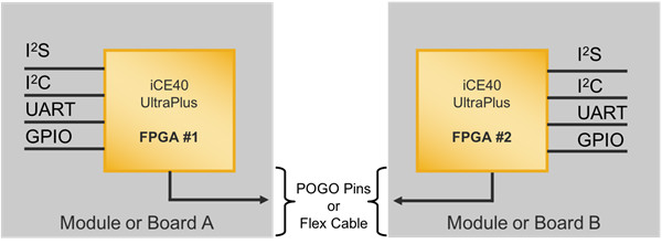
Single-Wire Aggregation (SWA) IP allows developers to aggregate up to seven I2C, I2S, GPIO, and/or DisplayPort Auxiliary (DP-AUX) transmission/receive (Tx/Rx) signals into one single-ended connection, reducing the number of physical board-to-board or component-to-component connectors required in a given design. Aggregating multiple signals in a single wire and then deaggregating them on the other end minimizes system size and cost, simplifies PCB signal routing and integrity issues, and eliminates connector hardware that, according to Lattice, is “the single highest contributor to system reliability.”
SWA IP targets Lattice iCE40 UltraPlus FPGAs and uses bi-directional, time-division multiplexing-based (TDM-based) communications to link boards and components. The use of variable-length packets allows the IP to optimize communications bandwidth, and Rx-side parity error detection enables a retransmit characteristic for I2C and GPIO communications. GPIOs can also recognize I2C interrupts thanks to an event-based transmission feature.
SWA IP supports raw data rates of 7.5 Mbps or higher. I2C packets are carried at 100 kbps, 400 kbps (fast-mode), or 1 Mbps (fast-mode plus). Two I2S data channels are supported, and an optional I2S controller allows I2S Tx devices to generate SCK and WS signals.

A DP-AUX channel supports data payloads of up to 152 bits.
SWA in Action
The SWA requires a pull-up resistor on the order of 200Ω to sustain the link. The iCE40 UltraPlus FPGA’s internal oscillator can be used to generate a 24 to 60 MHz clock for the SWA IP. For designs leveraging I2S communications, an external clock is required.
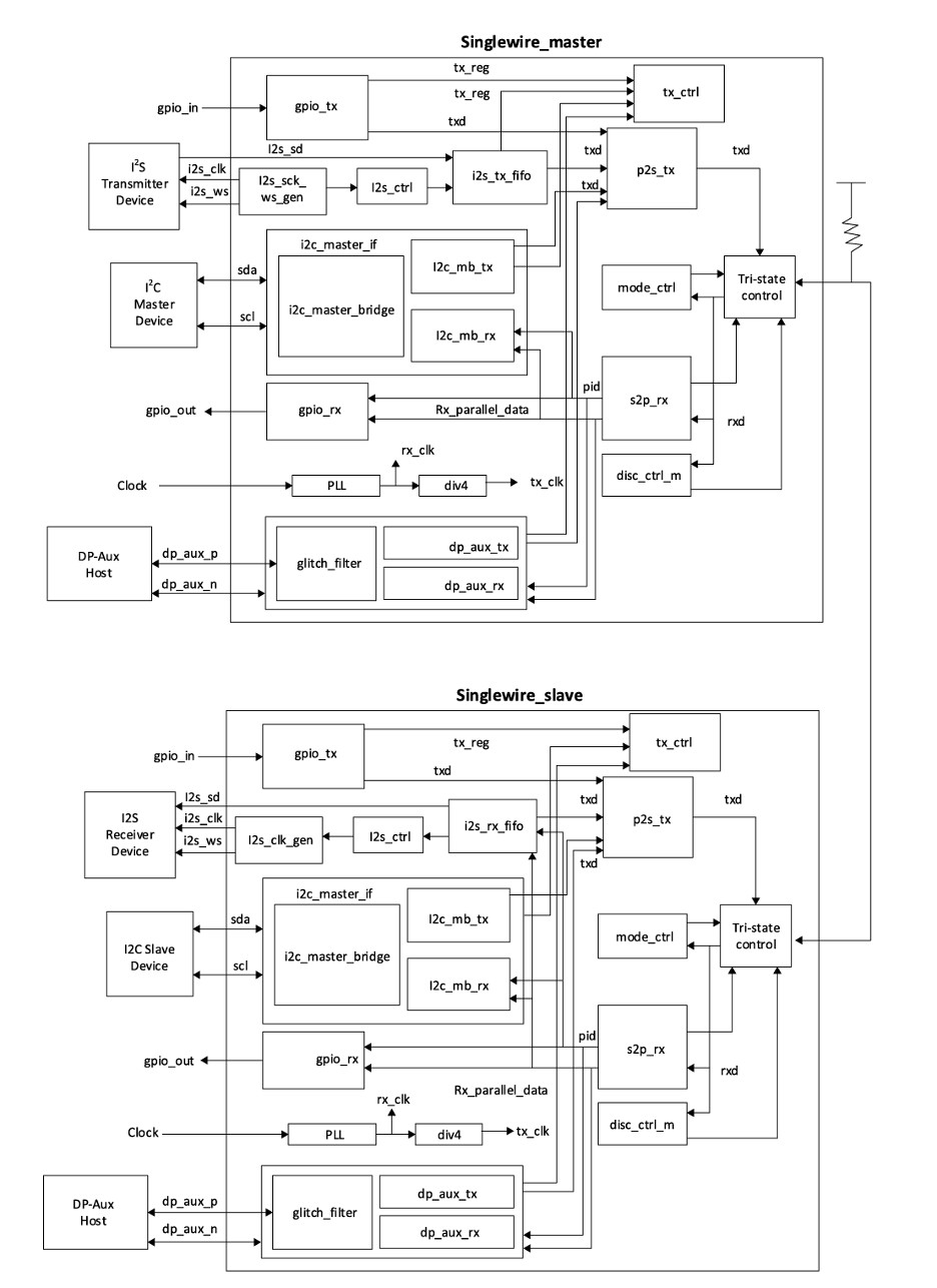
The diagrams below show an SWA reference design comprised of both a Master and Slave FPGA. In operation, the Master would send a low pulse across the single-wire connection, and wait for an acknowledgement pulse back from the Slave. If I2S communications were being used, the Master would then send an I2S SCK pulse for Slave FPGA clock training.

Users can configure, compile, and generate a bitstream for the SWA IP using Lattice Radiant development environment. Source code is available and expanded parameterization is supported so that development teams with hardware description language (HDL) expertise can customize the IP for their particular use case, for example by combining Lattice SWA bitstreams into their own HDL code.
However, for design teams without HDL experience, Lattice provides pre-configured SWA bitstreams in the following I/O configurations:
- One I2C Controller, One I2C Peripheral, One I2S, and Eight GPIO Signals
- One I2C Controller, One I2C Peripheral, Two I2S, and Eight GPIO Signals
- Six I2C Controllers and Two GPIO Signals
- One I2C Controller and 12 GPIO Signals
- Three I2C Controllers, Two I2C Peripherals, and 15 GPIO Signals
Beyond these popular configurations, customers can source other custom bitstream configurations from Lattice free of charge.
Getting Started with SWA IP
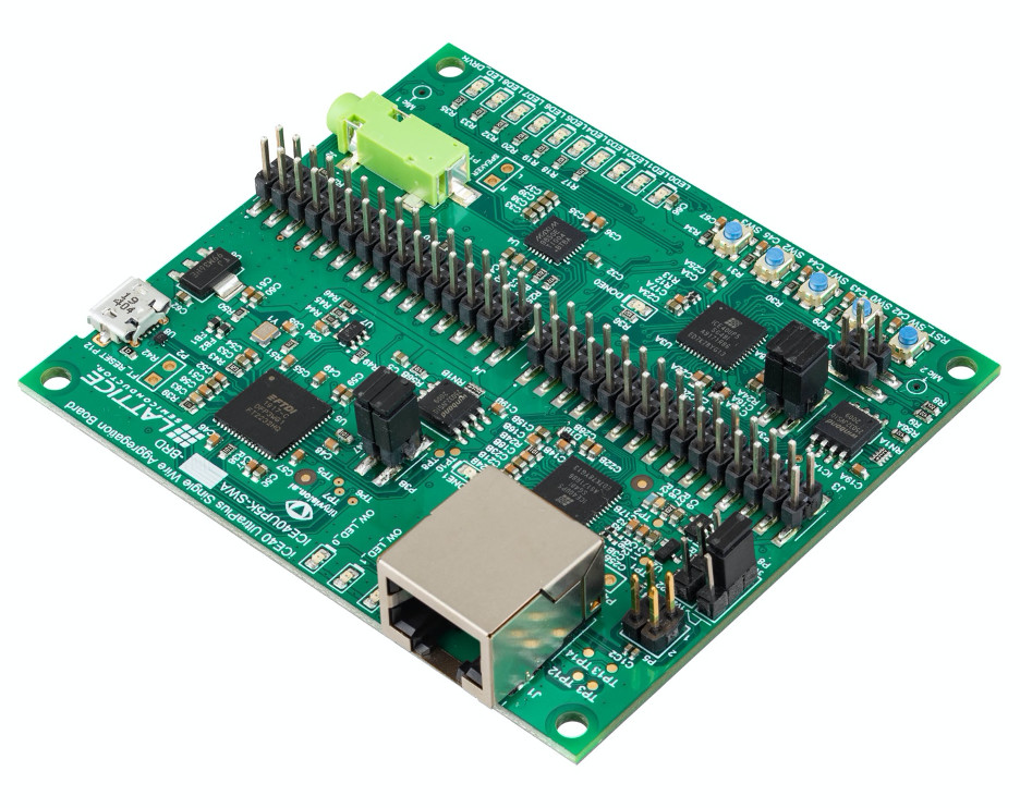
Developers interested in using SWA IP to reduce the cost, size, and PCB complexity of their embedded designs, while potentially improving system reliability, can evaluate the technology through the Single-Wire Aggregation Demo/Development Board (part number iCE40UP5K-SWA-EVN). It is available for $249, and is provided with ample documentation, source code, and how to/getting started videos.
With the board, engineers can verify the aggregation of multiple I2c and GPIO signals. I2S signals can be verified using the iCE40 UltraPlus Mobile Development Platform (MDP), and DP-AUX signals can be verified in simulation.
For more information on SWA IP, consult the video overview embedded below or follow the resource links at the bottom of the page.
- Single Wire Aggregation Overview: https://www.latticesemi.com/singlewire
- Single Wire Aggregation Development Board & Resources: https://www.latticesemi.com/Products/DevelopmentBoardsAndKits/SingleWire
- iCE40 UltraPlus Family Overview: https://www.latticesemi.com/en/Products/FPGAandCPLD/iCE40UltraPlus
- Lattice Radiant Software: https://www.latticesemi.com/Products/DesignSoftwareAndIP/FPGAandLDS/Radiant
- Lattice Website: https://www.latticesemi.com/


