
Improving Semiconductor Manufacturing Through Smart Technologies
October 27, 2020
Story
Internet of things (IoT) devices have become the largest driver of semiconductor revenue, with wireless communication, automotive, and artificial intelligence products following in short order.
Semiconductor manufacturing facilities are unlike any other. They can hold hundreds of millions of dollars in investment in some of the smallest products ever made by humans for commercial use. So small that a fleck of dust can cause irreparable damage to the final product. Over the decades, the industry has pioneered many groundbreaking procedures that other industrial manufacturers eventually would adopt decades later. And demand for these thin wafers is only expected to grow as more products, devices, and systems become reliant on computing power and complex nanostructures to operate.
But, this differentiation from the rest of the industrial manufacturing world is inexorably becoming a pressure point for seemingly never-ending innovation in operations to achieve ever higher investment returns. Many of the improvements made in the last few decades have been highly valuable, but their success has created a journey of diminishing returns. These improvements were often made in the name of higher yields. A crucial metric, no doubt, but concentrating on a single factor of optimization can lead engineers to design themselves into a corner. From this position there have historically been two options; invest in smaller nodes or larger wafers. Both of which are lucrative, but require billions of dollars in upfront capital investment.
This makes it nearly impossible for all except the largest foundries and fabricators to compete. Here is where smart manufacturing comes in. At the simplest level, all manufacturing facilities have three adjustment knobs to turn: cost, time, and quality. What smart manufacturing does is improve the fine adjustments on these three knobs, allowing greater control over the enterprise. There are other benefits, like rule-based planning and process optimization, positioning smart manufacturing as a welcome path out of the diminishing return corner.
A new age of IC development
Increased growth
Internet of things (IoT) devices have become the largest driver of semiconductor revenue, with wireless communication, automotive, and artificial intelligence products following in short order1. This broad array of devices will bring far more variation to the industry, but optimizing manufacturing for such a diverse range of products will become an even greater hurdle. What will be the best schedule to produce all these different products? Is production going to be treated like a black-box with no knowledge of what’s happening in real time? What if a change needs to be made to a design -- how long will it take to adjust the process? And will production efficiencies be comparable to before the change?
Track and trace requirements
Many semiconductor applications are also taking on more important safety-critical roles in society, responsible for the wellbeing of human lives. To cope with this new risk to the OEMs, many businesses want or require strict track and trace protocols. If an advanced driver-assist feature in a new car malfunctions earlier than expected, detailed process information will be invaluable in finding the root cause. Other applications like security and biometrics need an assurance that none of the design has been altered or tampered with during fabrication. And a growing segment of the consumer electronics market has an interest in the sustainability of the products they purchase. How can a customer know what they received is what they purchased?
Yield optimization is getting harder
Yield is undoubtedly a key metric to optimize profitability, but so much of this process is already being automated and optimized—especially at the largest fabs and most advanced nodes. Smart manufacturing is not just a secondary route for optimization, it is a cartographer mapping all the other possible paths for improving efficiency and profitability, and testing their efficacy before ever changing a sensor in a fabrication facility.
The path to success
The value of smart manufacturing is in its flexibility, a core component of Siemens’ Xcelerator portfolio of software, services, and application development platforms to bring organizations new insights, opportunities and automation. When producing at massive scales, even small tweaks to processes can net huge savings. To illustrate the importance of this approach in driving innovation, two examples will be discussed - lot size optimization and scheduling optimization.
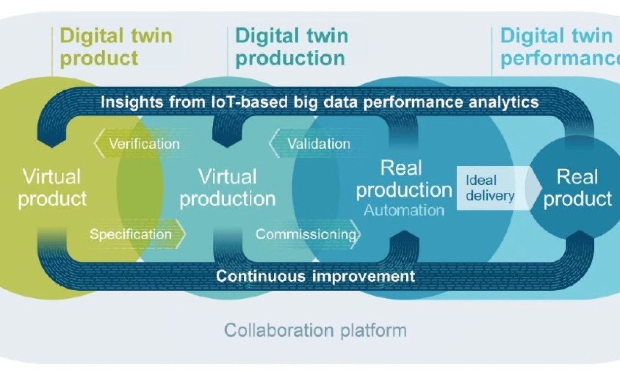
“Digital twins can be of product, production, or performance. Ideally, these digital twins feed each other for insights and continuous improvement. Siemens Xcelerator portfolio of products covers the design, realization, and optimization of digital twins,” said Alan D. Porter, Vice President of Electronics & Semiconductor Industry at Siemens Digital Industries Software.
Suppose a new fabrication facility is being built with an investment of nearly $14 billion. The first 60 days of operation yield 100,000 viable IC units out the door. Off the top, about 25 percent of that is going to be moved directly to storage. That is a lot of investment to leave in a room, but this is a common occurrence across the industry.
25 percent of $14 billion is a vast amount of lost savings, especially compared to the returns of an increased yield of a quarter of a percent ($20 – 40 million). Why does this occur? Because many companies do not have sufficient visibility into the precise details of their fabrication facilities.
Lot size optimization
Like many other disciplines, semiconductor fabrication can fall victim to tradition. Most fabs producing wafers smaller than 300mm run lot sizes of around 25 wafers, though smaller lot sizes may be more efficient in certain circumstances. But lot size optimization is not concerned with these metrics. Instead it focusses on the number of die needed to assemble multi-chip modules from these wafers.
As an example, an IC package may include a processor die that derives from a primary wafer that holds 10,000 die. A complimentary wafer of memory die may have 15,000 die. Typically, 10,000 multi-chip modules would be built to match the primary die quantity because that is the norm and they are the more expensive die. That leaves 5,000 extra memory die. What happens to this excess? Often they are stored somewhere in the facility, where they languish and possibly expire or get lost in storage. Eventually, the loss is taken as a yield loss. This can result in millions of dollars’ worth of complimentary die simply being lost or scrapped.
That’s a sizable amount of money. But, it’s not the full value lost. Those die had to be made, taking up manufacturing capacity. And they went through assembly, using more valuable resources until they are eventually stored on a shelf and hard to find. There are still more losses though -- 10,000 die per primary wafer was just what would fit. The order may have been for only 8,000 units, but the primary die are expensive so they were overbuilt by 20 percent.
In our experience with semiconductor manufacturers around the world, this is a conservative estimate. Many fabs routinely overbuild by 30 percent. Yes, some of the overstock can be sold later, but what if there was a mid-cycle revision? That leaves about 15 percent of the total as lost revenue.
Die level traceability
Many products may also require traceability to know when a die went through production, what the conditions were or if there is a higher failure rate in that lot. But to fully optimize lot sizes and scheduling, a more precise tracking method is needed: die level traceability. Tracking a single die through production, into assembly and out into the real world eliminates many of the hurdles to efficient and profitable production.
Scheduling optimization
To increase operational clarity, a few processes need to be established:
- First, a finite scheduling system is needed. One that understands everything that’s going on, in real time. But this requires a digital transformation. Ready access to data about every process on the production floor gives much greater insight to overall efficiencies but is nearly useless without a continuous digital thread that spans from the machines and workers to management and control processes.
- Second, to establish the digital thread for a finite scheduling system, IoT sensors need to be aggressively deployed throughout the fabrication facility. Fortunately for many fabs, their machines may already be generating enormous amounts of data. This includes highly accurate temperature and humidity readings to ensure a stable and optimal production environment for the semiconductors. It can even include the speed of servos within the machines or the force required to hold wafers.
- The last requirement is that the entire factory floor needs to be simulated accurately. How do theoretical process times compare to actual times? What about individual steps in the process? How long does it take to switch tools? To make these answers converge and enable optimization, real world data from the IoT infrastructure needs to be fed back into the simulation model. This creates a closed-loop model that makes it possible to eventually support advanced AI capabilities such as machine learning.
These three steps make production faster and more efficient. But there is one more crucial factor: lot size optimization. If the four steps are implemented without this capability, the storage rate will only grow, as production will outpace demand even more than before.
Conclusion:
Production yields are a great metric, but they are not the only metric for an efficient semiconductor fab, especially as the market is only expected to grow in capacity and complexity. Failing to look at other processes beyond literal production leaves millions of dollars either sitting in a storeroom, or even worse, at the bottom of a trash can. Smart manufacturing is meant to widen the scope of interest when optimizing a factory. As part of Siemens’ Xcelerator portfolio, the tools for semiconductor development and production are bringing tomorrow’s production efficiencies to factories today.
Sources
1)2019 KPMG International Corporation, 2019 Global Semiconductor Outlook: Semiconductors: As the Backbone of the Connected World, The Industry’s Future is Bright
About the Author
Alan D. Porter is Vice President, Electronics & Semiconductor Industry at Siemens Digital Industries Software. He joined Siemens in 2020 having completed over 30 years in the semiconductor and electronics engineering environment across multiple industries, including consumer electronics, mil/aero, automotive, and network infrastructure. He worked in large corporations including Apple and Huawei, EDA software companies including Mentor, Synopsys and Cadence, start-ups and professional services roles for high and low volume products.


