
Execute in Place (XiP): An External Flash Architecture Ideal for the Code and Performance Requirements of Edge IoT and AI
September 19, 2019
Story

Emerging applications and use cases are disrupting Traditional MCU architectures' design paradigm with evolving system requirements that demand a lot of code and processing.
Traditional microcontroller (MCU) architectures—featuring a processor, on-chip flash memory, and peripheral input or output devices—have remained mostly unchanged for over 40 years. However, emerging applications and use cases are disrupting this long-established design paradigm with evolving system requirements that demand:
- A lot of code and/or
- A lot of processing and performance
For instance, consider the proliferation of small, connected devices such as IoT endpoints or wearables that run advanced cellular or wireless protocols like LTE-M, NB-IoT or Wi-Fi. These communication stacks contain a great deal of code and won’t typically fit in an MCU’s embedded flash memory due to the sheer size of the application software.
Or consider the rapid growth of artificial intelligence (AI) and inferencing applications that require substantial amounts of data processing performance at the network edge, which in turn can drive high levels of power consumption. To address these dual, competing requirements for more performance and greater power efficiency, designers can build their designs on more modern process technologies, such as 22nm or even finer geometries. However, these newer process nodes aren’t offered with on-chip flash.
These use cases present a challenge for edge device designers: how to design an architecture that provides the needed performance and memory space to execute a substantial amount of code while observing the constraints of extremely low power consumption and ever-smaller chip footprints.
An Architecture for Memory Expansion
The answer is to place some or all of the MCU flash memory off-chip, operating in Execute in Place, or XiP mode. XiP is a method of executing code directly from external flash memory rather than copying it first from the flash to RAM and then executing the program from that RAM. Because the flash memory in an XiP architecture is external to the chip, designers aren’t constrained by the amount of memory that will fit on the die -- the external memory can be as large as necessary to efficiently process even very large code sets.
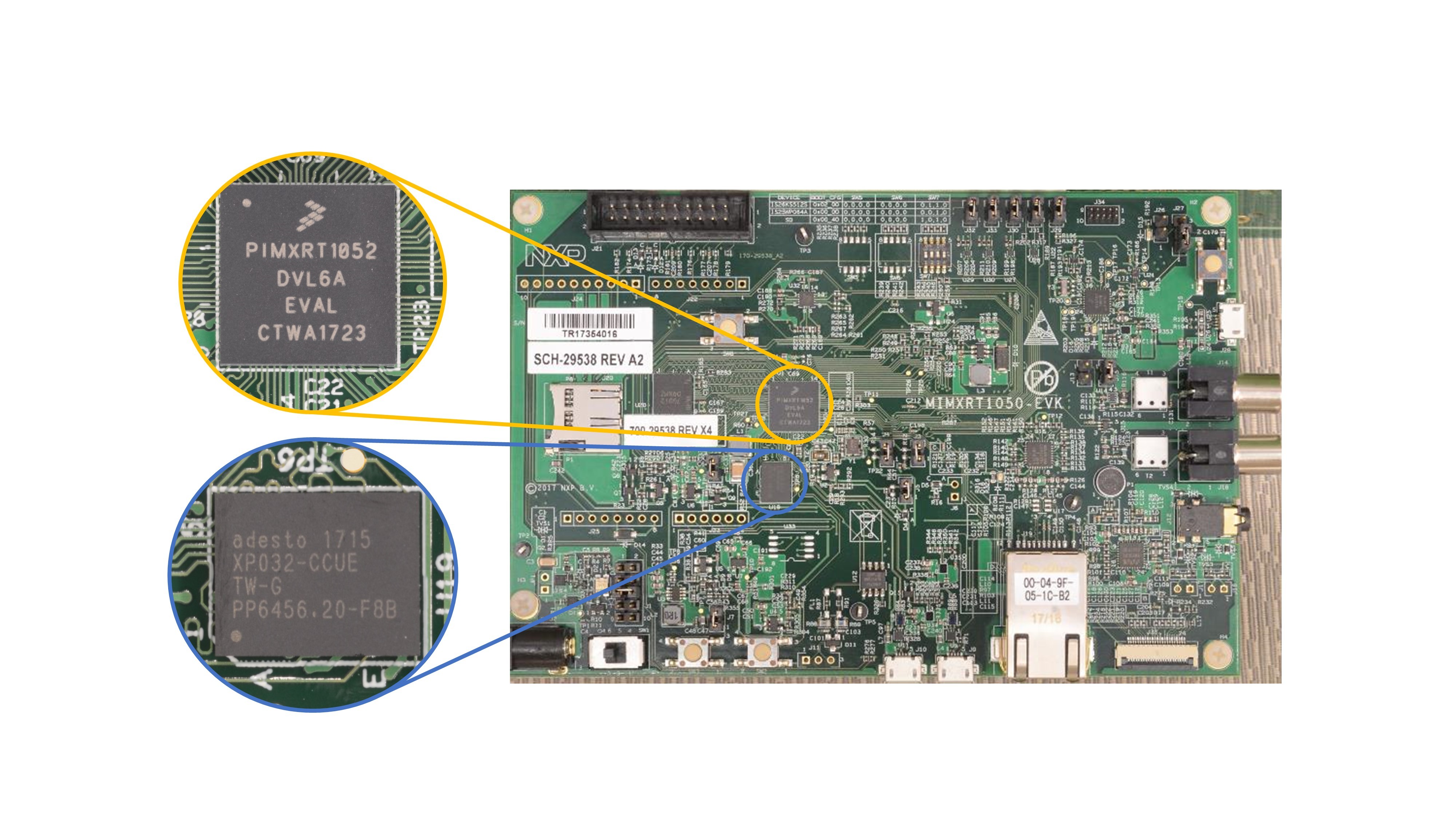
A leading example of this new MCU architecture is the RT family of “crossover processors” from NXP, such as the i.MX RT1050. Design flexibility is one of the major advantages of these devices, as they don’t include internal flash memory and instead use external memory, which allows these MCUs to accommodate any size of code and data memory space as required by the application. Also, by removing embedded flash from the chip, NXP is able to place other features on the die to help optimize for improved performance or power efficiency.
Placing the flash memory off-chip also enables the manufacturing of processors in more advanced process nodes (below 40nm) to support higher processing speeds, greater power efficiency, and lower costs. Embedding flash is challenging, particularly with modern process technologies, and the additional manufacturing steps needed to embed flash significantly increases the cost of silicon. MCUs designed with on-chip flash must absorb the costs of the process – about 30 to 40 percent more expensive than the same version of that process without flash – as well as the area cost of the flash itself.
However, to make a successful XiP architecture, designers can’t just use any flash memory. Serial flash memory is typically used for application program storage, such as BIOS in a PC. For this purpose, the performance or power efficiency of the flash memory module isn’t particularly important, as it’s only used at boot-up to copy the contents of the flash to RAM. However, when flash memory is used in XiP architectures, software is fetched from external memory on-demand, meaning that high performance and power efficiency become critical.
Adesto has designed a flash memory device that is specifically optimized to operate as an external memory for XiP microarchitectures. Adesto EcoXiP Octal xSPI non-volatile memory (NVM) takes advantage of advancements in serial flash technology to meet high performance requirements, enabling flash devices to respond with random access to read requests from devices like the NXP RT1050 and deliver instructions and data with low latency and high throughput.
Flash Memory Challenge No. 1: Performance Bottlenecks
Building an external flash memory system to operate as random access memory in XiP architectures present a number of challenges. First, the processor and the external flash memory are separate devices, connected by a serial bus interface. In a traditional serial interface, data are transferred serially, over a single line at a time. This introduces performance bottlenecks and data flow latencies, particularly in systems with high performance requirements.
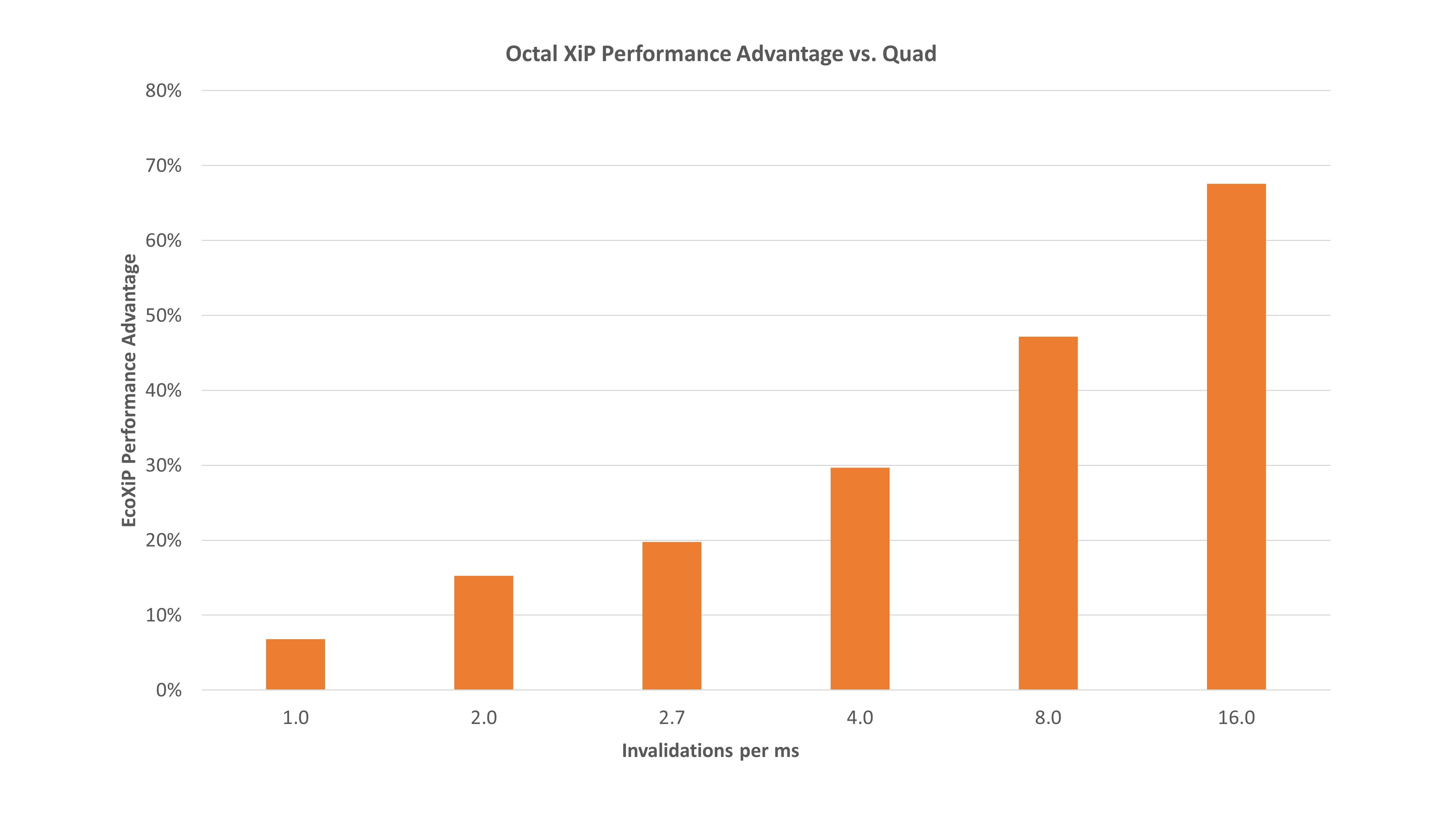
Adesto designed EcoXiP to respond quickly to read requests from the host MCU and deliver instructions and data with low latency and high throughput. In fact, EcoXiP devices are compliant with JEDEC’s latest Octal SPI protocol (xSPI), making the communication much faster than a single wire serial flash. EcoXiP offers multi-line, smart serial peripheral interfaces to speed data flows between the CPU and external flash memory, allowing data to transfer over eight parallel data lines at a time.
In addition, EcoXiP features double data rate (DDR), a capability that is common in high-speed DRAM. DDR works by sending data bits on both the rising and falling edges of the serial clock. Modern serial flash devices deliver clock speeds greater than 100MHz, and since it takes only half a clock cycle to send out a data bit, DDR has the potential to double the throughput from the external memory. Combining the Octal interface with the DDR capability increases the throughput of xSPI protocol over single-wire serial flash by a factor of 16X.
EcoXiP also addresses latency by reducing the overhead of the command interface. The “continuous” mode of the Burst Read with Wrap command allows faster access to data by reducing the number of clock cycles needed for subsequent reads of data. Employing this command eliminates the need to send a command and address, then wait for the array access time (dummy cycles) in consecutive cache misses. This can save about 20 cycles in such accesses, reducing the average latency as seen by the CPU.
Flash Memory Challenge No. 2: Power Efficiency
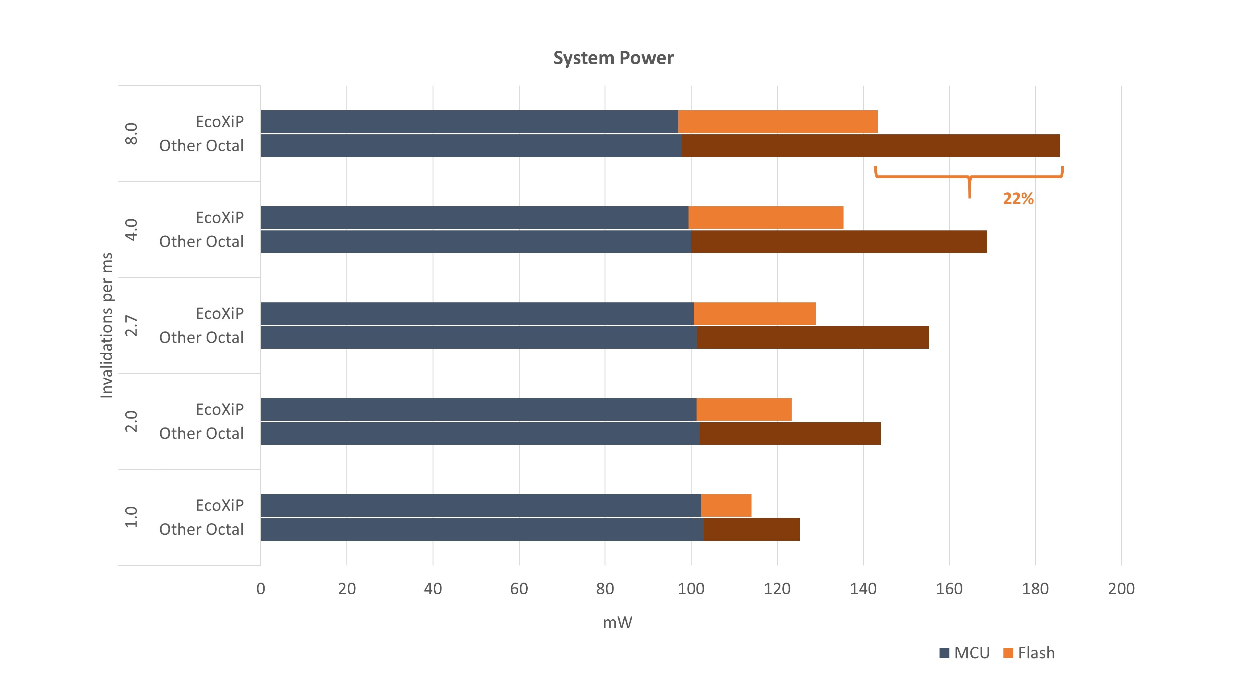
Another challenge in building an XiP system with discrete CPU and external flash memory is that powering these two separate devices, in addition to the energy required for the intercommunications, may increase a system’s total energy consumption. The design of EcoXiP mitigates this risk by offering competitive power consumption while in XiP mode. For 133MHz Octal SPI reads, the EcoXiP read current is typically 35mA – about half the rate of similar Octal SPI devices. In addition, EcoXiP offers configurable strength I/O drivers. Optimizing the strength of the drivers minimizes the power consumption required for the communications between the CPU and EcoXiP.
In addition, EcoXiP offers deep power-down and ultra-deep power-down modes for times when the CPU does not require the flash. While in ultra-deep-power-down mode the device typically draws 200 nanoAmps – resulting in extremely low power consumption with only a small impact to wake-up time.
The ultra-deep-power-down mode offers another advantage of XiP over RAM-based systems. The power consumption of the flash in that mode is significantly lower than that of either on-chip SRAM or external DRAM. Some RAM-based system designers would choose to turn off the power to the memory while in deep-sleep, but that would require reloading the RAM from an external flash, a time- and power-consuming operation.
Flash Memory Challenge No. 3: Over-the-Air Updates
Another challenge faced by designers of XiP systems is providing a way to perform over-the-air (OTA) updates to program information on the external flash memory. Writing to the flash with an OTA update can block the flash from responding to reads for an extended period of time, preventing the next instruction that the system needs for the update, resulting in a processing deadlock.
EcoXiP’s concurrent read-write, also known as read-while-write or RWW, allows the host processor to continue reading from a partition of the flash memory array while modifying data on another part. As an example, periodic data logging that involves erase and program operations to the serial flash does not put the XiP program on hold. With the RWW feature, instruction and data fetching during programming continues as usual in a different partition of the flash.
Adesto has worked closely with JEDEC, the global leader in developing open standards and publications for the microelectronics industry, to establish standards for how MCUs communicate with serial flash devices in an XiP architecture. Adesto is the first flash manufacturer to implement all the serial flash JEDEC standards including JESD216D, JESD251 and JESD252, so designers who adhere to these standards can dependably implement EcoXiP to build advanced devices that are optimized for XiP architectures.
Conclusion
While off-chip flash is not the answer to every challenge that chip designers face, or even the answer for every system or application, an XiP architecture offers the ability to support expandable amounts of external software and data memory space for emerging use cases, particularly for edge IoT and AI applications. Employing external serial flash memory in conjunction with an embedded processor delivers a highly scalable platform that aligns to many of the challenges of today’s evolving embedded systems.
Gideon Intrater is Adesto’s Chief Technology Officer. He brings more than 30 years of experience in the semiconductor market to his role in the company. Gideon serves on the Advisory board of Centipede Semi and Think Silicon and was previously a member of the advisory board of Sansa Security (acquired by ARM in July 2015). Previously, Mr. Intrater was Vice President of Marketing at MIPS Technologies (until the company was sold in February 2013). Before joining MIPS, Mr. Intrater was Vice President of Architecture for Symwave, a privately held supplier of high-performance analog/mixed signal semiconductor solutions for consumer devices. Prior to Symwave, Mr. Intrater held various management positions at MIPS Technologies and National Semiconductor Corporation. Mr. Intrater holds over 30 issued patents. He earned BSEE and MSEE degrees from the Technion, Israel Institute of Technology, and an MBA from San Jose State University.


