
Breakthrough, Scalable, Intuitive Power Sequencing System Accelerates Design and Debug
October 08, 2020
Story
It's no secret that electronics systems are becoming more complex across all industries. It is less obvious how this complexity has infiltrated power supply design.
Introduction
It’s no secret that electronics systems are becoming more complex across all industries. It is less obvious how this complexity has infiltrated power supply design. For instance, functional complexity is commonly addressed by using ASICs, FPGAs, and microprocessors to enrich application feature sets in ever-smaller form factors. These devices present disparate digital loads to the power system, requiring a wide variety of voltage rails over a range of power levels, each with highly individualized rail tolerances. Likewise, correct start-up and shut-down sequencing of the supplies is important. The multiplying of the number of voltage rails on a board has made power system sequence design and debug exponentially more complicated over time.
Scalability
The number of voltage rails required by an application board is a function of the board’s complexity. A power supply designer may face boards requiring only 10 voltage rails, as well as those requiring 200 voltage rails. Sequencer devices usually top out around 16 rails and are designed to easily be applied up to that number. Once the number of rails goes beyond that supported by a single sequencer, the complexity quickly increases, requiring designers to learn the vagaries of each sequencer, and how it can be combined in complex systems.
Often, multiple sequencers are cascaded in high count voltage rail systems, a nontrivial task. In a cascaded system, complexity increases exponentially with a linear increase in the number of voltage rails. Designers have adopted creative methods of cascading sequencers to mitigate complexity, such as using ping-pong mechanisms or sharing the fault and power good status via dedicated digital signals. While these solutions suffice in relatively straightforward sequences, they quickly become untenable in systems that deviate from simple power-up/power-down sequencing.
The ADM1266 solves the problem of complexity with true scalability. It is the latest addition to ADI’s Super Sequencer® family of parts. Connecting multiple ADM1266 devices requires the use of a dedicated two-wire interdevice bus (IDB) to communicate. Each ADM1266 is capable of monitoring and sequencing 17 voltage rails, and up to 16 ADM1266 devices can be connected in parallel to monitor and sequence 257 voltage rails, as long as all devices are connected to the same IDB.
The ADM1266 uses a single master with additional ADM1266 devices acting as slaves. The devices use a parallel architecture in which every single ADM1266 connected to the IDB transitions to the same next state, depending on system conditions, ensuring that every ADM1266 on the bus is in sync. Bus communication is transparent, so the designer’s experience is the same in creating a sequence for a single ADM1266 as it is for 16 ADM1266 devices. A significant advantage to this system is that designers only need to learn how to use one device for both simple and complex designs, eliminating multiple learning curves for different devices. Cascading multiple devices is as simple as connecting them to the same IDB, as shown in Figure 1.
Event-Based Sequencing
Modern sequencers must do more than just monitor voltage rails, they must also react to digital signals. Traditional time-based sequencers have fixed signals with a dedicated outcome and limited functionality.
Let’s take an example of a motherboard with an optional daughter board. A daughter card detect signal is monitored by the sequencer: when this signal is present, the sequencer brings up the voltage rails present on the daughter card; when the signal is not present, the sequencer continues with the motherboard sequence procedure, finishing with the power in good state. Such a daughter card detect signal is not available on most traditional sequencers. Additionally, such requirements change based on the application, and can be addressed with general-purpose input output pins (GPIOs).
Another example involves powering an ASIC and an FPGA wherein the system requires that the ASIC be completely powered up and running before the FPGA is powered. In this case, the sequencer brings up the ASIC supplies in order, then waits for a digital power-good signal from the ASIC. Once the ASIC power good signal is asserted, it waits 100 ms before it continues to power the FPGA. An event-based sequencer is required to produce this complex sequence. In a system with multiple sequencers, it is important that the event information on one device is shared with the other devices on the board so that they act in unison.
Voltage monitor OV and UV comparators, digital signals like GPIOs and PDIOs, timers, variables, and messages from the IDB all feed into the feature-rich ADM1266 sequence engine and trigger events. The user can easily create complex state machines that monitor a variety of events and take appropriate actions.

Figure 1. It is easy to scale up a sequence with multiple ADM1266s by combining them via an IDB.
Accelerating System Design
Traditionally, the user experience of designing a power sequencing system using a single sequencer is vastly different than that for a system requiring multiple sequencers. That is, a design with a single sequencer for 16 voltages is often straightforward: the designer uses a software graphical user interface (GUI) to configure each voltage rail and their sequencing. The process is generally a manual selection/setting process repeated for 16 rails. Now imagine a design with five sequencers and 80 rails. Manually configuring 80 rails using a GUI is time consuming and prone to human error. The designer must also determine how to best cascade multiple devices and assign the resources of the five sequencers to the 80 voltage rails. Most software-assisted design tools do not actually assist. The user must understand the specific functions of the sequencer IC and explicitly tell it what to do via the GUI, creating a fairly steep learning curve for each project.
The ADM1266 takes a different approach. It is configured and debugged using PC-based ADI Power Studio,™ which does far more than configure the various settings of the ADM1266. ADI Power Studio is a complete development and debugging tool that assists the designer in realizing a robust sequence. It enables the designer to approach the power system at a much higher level than traditional GUIs. For instance, built-in wizards enable the designer to set up and configure 80 voltage rails in a few minutes, a task that would take a few hours if done manually. Figure 2 and Figure 3 show some examples of the interface.

Figure 2. ADI Power Studio features custom rail names, which can greatly

Figure 3. One step configuration of an entire system. The system rails wizard leads the designer through the process of configuring an entire sequence using the same interface regardless of the rail quantity. Note the user-defined custom rail names, making it easier to recognize individual rails on sight.
The designer starts by creating a virtual state machine to meet the requirements for the system. In a single sequencer design (≤17 rails), the virtual state machine of the GUI simply matches the state machine of the sequencer. As more sequencers are added, the virtual state machine deviates from the individual sequencer state machines, requiring additional steps in the state machine as devices communicate various events with each other.
For example, a designer monitors two voltage rails on Sequencer 1 and two voltage rails on Sequencer 2. The design requires that if any of the four voltage rails sees a fault, then everything shuts down. In practice, since there are two devices, they will have to share a fault signal between them. The system’s virtual state machine and the state machines for the individual devices are shown in Figure 4.

Figure 4. Virtual state machine vs. device-level state machine.
As the number of rails and the sequencing requirements become more complex, the system’s virtual state machine and the state machines at the device level increasingly deviate. The designer knows what he or she wants to happen, but must make the sequencers work together to make it happen, a time consuming and usually buggy process. ADI Power Studio automates much of the state machine creation process. The user designs the virtual state machine using the GUI, while the compiler in the ADI Power Studio handles the complexity of communicating between various sequencers. This enables the designer to create complex state machines using a flexible, intuitive process.
Powerful Debugging Tools
Bugs naturally occur throughout the development of any complex system. Ideally, most bugs appear and are eradicated during development, but some creep into production. Either way, it is critical that system designers have the tools to quickly identify failures and make changes to address them, as a designer usually spends significantly more time debugging than in pure design. Typical failures consist of failed voltage rails and signals at wrong logic levels.
Let’s continue with the example of bringing up a board with 80 voltage rails, where it is not uncommon for one of the rails to fail in the design phase. Failure can be a design flaw at the component level or at the configuration level. Either way, identifying the problem begins with identifying the troublesome rail. The problem is that in a typical sequence, if any voltage rail fails, then the sequencer shuts down all voltage rails. This shutdown behavior, although robust in a production-level product, gets in the way of debugging during the design phase, as the failure is hidden by the failure of the entire system. The designer cannot see the tree for the forest. It is unlikely that a designer can concurrently benchtop monitor all 80 rails, making it nearly impossible to identify the guilty rail as it fails.
In an ideal debugging system, once a failure-prone voltage rail is identified, other voltage rails remain powered so that the behavior of the problematic rail can be observed while the rest of the system remains active. Although forcefully modifying the sequence configuration can achieve this goal, breaking the sequence to debug the sequence is a cumbersome approach at best.
ADI Power Studio and the ADM1266 feature advanced debugging tools are commonly found in software design environments to simplify the debugging process. The first debugging tool comes in the form of breakpoints, where the sequence stops progressing at a particular state. In a system with multiple ADM1266 devices, all ADM1266 devices will transition through the state machine and stop at the beginning of the state for which has the user-defined breakpoint. This pause in the sequence enables the designer to debug the failing voltage rail or verify why the signal is not at its correct logic level.
A designer can also step through a sequence by applying breakpoints to all states. One application of single stepping is to check pre-bias startups for voltage rails before they are enabled. A designer can single step through the power sequence to see if any presumably disabled rails have voltages at their outputs—shown in the monitor window section of ADI Power Studio. Figure 5 shows an example of user-defined breakpoints.

Figure 5. Breakpoints enable the designer to pause the sequence at any state for enhanced debugging.
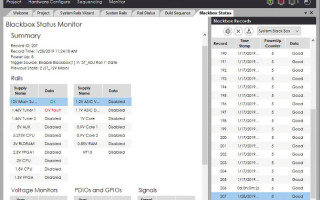
Another debugging tool is the blackbox recording feature, where the ADM1266 takes a snapshot of the status of all the voltage monitoring and digital pins when triggered by a critical event. Once a blackbox is triggered, it records information such as the state when the event happened, the previous good state, the time of the event, the number of times the part has powered up and seen a fault, etc. This helps the designer pinpoint failures and quickly diagnose causes.
The blackbox feature plays a critical role in capturing fault conditions in production application, assisting in maintenance and upgrades. It can also be used as a debugging tool in development. For instance, when a design is facing thermal chamber testing or mechanical testing, it can be impossible to probe using benchtop lab equipment, whereas blackboxes can capture failures for later review. Figure 6 shows a screenshot of a blackbox record.

Figure 6. Blackbox status monitoring takes a snapshot of conditions at user-defined events. Blackbox triggers can be included in production systems to aid in field troubleshooting and maintenance, as well as in debugging.
Conclusion
To address the increasing complexity of power sequencing requirements, solutions must be scalable, feature rich, and intuitive. ADI Power Studio and the ADM1266 17-channel sequencer meet these conditions with high-level design and debugging tools that reduce development and debug time. This enables designers to focus more time on innovation and producing robust solutions.
About the Author
Navdeep has worked at Analog Devices for 14 years, during which time he has been involved with breakthrough products like digital power and Super Sequencer® devices. He was the architect for an intuitive digital power graphical user interface, and most recently he was the architect for the ADM1266 Super Sequencer, overseeing the firmware, software, and hardware development. He has three patents and an M.S. degree in electrical engineering from San José State University. He can be reached at [email protected].


