
Introduction to the SPI Interface
December 30, 2019
Story

This article provides a brief description of the 4-wire SPI interface followed by an introduction to SPI enabled switches and muxes that help reduce the number of digital GPIOs in system board design.
The serial peripheral interface (SPI) is one of the most widely used interfaces between microcontroller and peripheral ICs such as sensors, ADCs, DACs, shift registers, SRAM, and others. SPI is a synchronous, full duplex master-slave-based interface. The data from the master or the slave is synchronized on the rising or falling clock edge. Both master and slave can transmit data at the same time. The SPI interface can be either 3-wire or 4-wire.
This article provides a brief description of the 4-wire SPI interface followed by an introduction to SPI enabled switches and muxes that help reduce the number of digital GPIOs in system board design.
The Interface
4-wire SPI devices have four signals:
- Clock (SPI CLK, SCLK)
- Chip select (CS)
- Master out, slave in (MOSI)
- Master in, slave out (MISO)
The device that generates the clock signal is called the master. Data transmitted between the master and the slave is synchronized to the clock generated by the master. SPI devices support much higher clock frequencies compared to I2C interfaces. Users should consult the product data sheet for the clock frequency specification of the SPI interface.
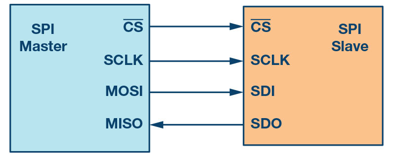
SPI interfaces can have only one master and can have one or multiple slaves. Figure 1 shows the SPI connection between the master and the slave.
The chip select signal from the master is used to select the slave. This is normally an active low signal and is pulled high to disconnect the slave from the SPI bus. When multiple slaves are used, an individual chip select signal for each slave is required from the master. In this article, the chip select signal is always an active low signal.
MOSI and MISO are the data lines. MOSI transmits data from the master to the slave and MISO transmits data from the slave to the master.
Data Transmission
To begin SPI communication, the master must send the clock signal and select the slave by enabling the CS signal. Usually chip select is an active low signal; hence, the master must send a logic 0 on this signal to select the slave.
SPI is a full-duplex interface; both master and slave can send data at the same time via the MOSI and MISO lines respectively. During SPI communication, the data is simultaneously transmitted (shifted out serially onto the MOSI/SDO bus) and received (the data on the bus (MISO/SDI) is sampled or read in). The serial clock edge synchronizes the shifting and sampling of the data. The SPI interface provides the user with flexibility to select the rising or falling edge of the clock to sample and/or shift the data (Refer to the device data sheet to determine the number of data bits transmitted using the SPI interface.).
Clock Polarity and Clock Phase
In SPI, the master can select the clock polarity and clock phase. The CPOL bit sets the polarity of the clock signal during the idle state. The idle state is defined as the period when CS is high and transitioning to low at the start of the transmission and when CS is low and transitioning to high at the end of the transmission. The CPHA bit selects the clock phase.
Depending on the CPHA bit, the rising or falling clock edge is used to sample and/or shift the data. The master must select the clock polarity and clock phase, as per the requirement of the slave. Depending on the CPOL and CPHA bit selection, four SPI modes are available. Table 1 shows the four SPI modes.
|
SPI
Mode
|
CPOL
|
CPHA
|
Clock Polarity in Idle State
|
Clock Phase Used to Sample and/or Shift the Data
|
|
0
|
0
|
0
|
Logic low
|
Data sampled on rising edge and shifted out on the falling edge
|
|
1
|
0
|
1
|
Logic low
|
Data sampled on the falling edge and shifted out on the rising edge
|
|
2
|
1
|
1
|
Logic high
|
Data sampled on the falling edge and shifted out on the rising edge
|
|
3
|
1
|
0
|
Logic high
|
Data sampled on the rising edge and shifted out on the falling edge
|
Figure 2 through Figure 5 show an example of communication in four SPI modes. In these examples, the data is shown on the MOSI and MISO line. The start and end of transmission is indicated by the dotted green line, the sampling edge is indicated in orange, and the shifting edge is indicated in blue.(Please note these figures are for illustration purpose only. For successful SPI communications, users must refer to the product data sheet and ensure that the timing specifications for the part are met).

Figure 3 shows the timing diagram for SPI Mode 1. In this mode, clock polarity is 0, which indicates that the idle state of the clock signal is low. The clock phase in this mode is 1, which indicates that the data is sampled on the falling edge (shown by the orange dotted line) and the data is shifted on the rising edge (shown by the dotted blue line) of the clock signal.

Figure 4 shows the timing diagram for SPI Mode 2. In this mode, the clock polarity is 1, which indicates that the idle state of the clock signal is high. The clock phase in this mode is 1, which indicates that the data is sampled on the falling edge (shown by the orange dotted line) and the data is shifted on the rising edge (shown by the dotted blue line) of the clock signal.

Figure 5 shows the timing diagram for SPI Mode 3. In this mode, the clock polarity is 1, which indicates that the idle state of the clock signal is high. The clock phase in this mode is 0, which indicates that the data is sampled on the rising edge (shown by the orange dotted line) and the data is shifted on the falling edge (shown by the dotted blue line) of the clock signal.

Multi-Slave Configuration
Multiple slaves can be used with a single SPI master. The slaves can be connected in regular mode or daisy-chain mode.
Regular SPI Mode
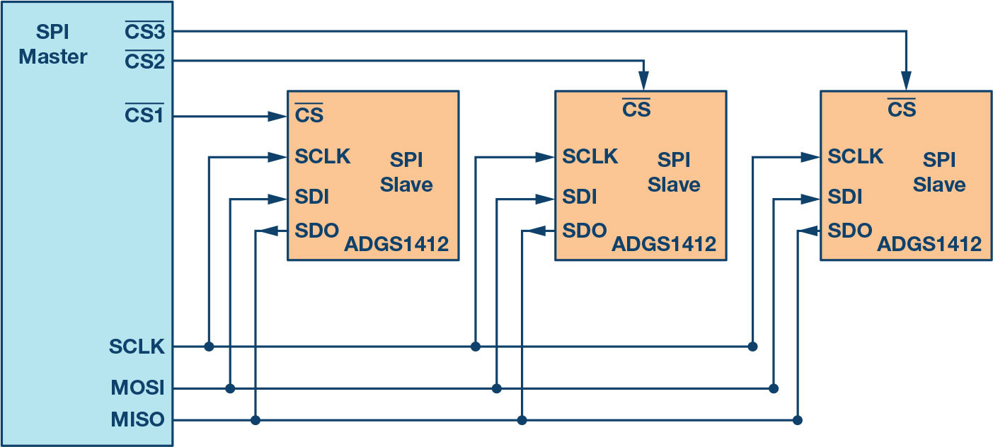
In regular mode, an individual chip select for each slave is required from the master. Once the chip select signal is enabled (pulled low) by the master, the clock and data on the MOSI/MISO lines are available for the selected slave. If multiple chip select signals are enabled, the data on the MISO line is corrupted, as there is no way for the master to identify which slave is transmitting the data.
As can be seen from Figure 6, as the number of slaves increases, the number of chip select lines from the master increases. This can quickly add to the number of inputs and outputs needed from the master and limit the number of slaves that can be used. There are different techniques that can be used to increase the number of slaves in regular mode; for example, using a mux to generate a chip select signal.
Daisy-Chain Method
In daisy-chain mode, the slaves are configured such that the chip select signal for all slaves is tied together and data propagates from one slave to the next. In this configuration, all slaves receive the same SPI clock at the same time. The data from the master is directly connected to the first slave and that slave provides data to the next slave and so on.
In this method, as data is propagated from one slave to the next, the number of clock cycles required to transmit data is proportional to the slave position in the daisy chain. For example, in Figure 7, in an 8-bit system, 24 clock pulses are required for the data to be available on the 3rd slave, compared to only eight clock pulses in regular SPI mode.
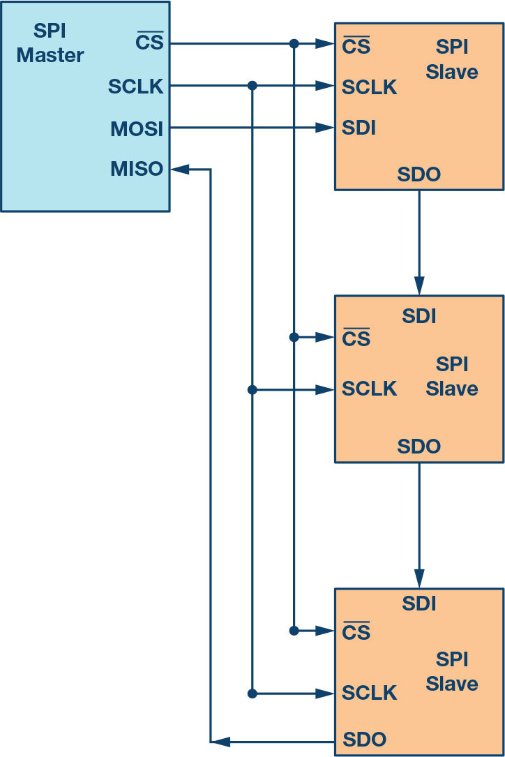
Figure 8 shows the clock cycles and data propagating through the daisy chain. Daisy-chain mode is not necessarily supported by all SPI devices (Please refer to the product data sheet to confirm if daisy chain is available).

SPI-Enabled Switches and Muxes
The newest generation of SPI enabled switches offer significant space saving without compromise to the precision switch performance. This section of the article discusses a case study of how SPI enabled switches or muxes can significantly simplify the system-level design and reduce the number of GPIOs required.
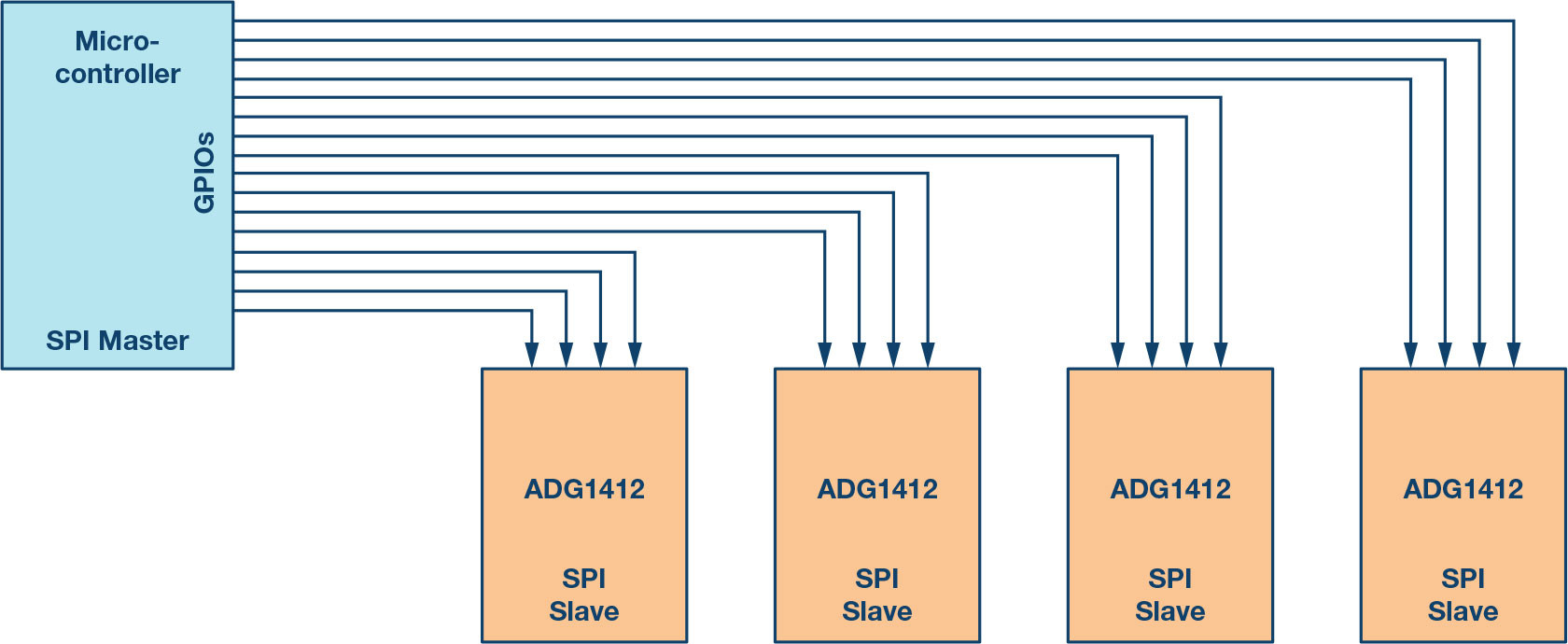
The ADG1412 is a quad, single-pole, single-throw (SPST) switch, which requires four GPIOs connected to the control input of each switch. Figure 9 shows the connection between the microcontroller and one ADG1412.

As the number of switches on the board increases, the number of required GPIOs increases significantly.
For example, when designing a test instrumentation system and a large number of switches are used to increase the number of channels in the system. In a 4 × 4 cross-point matrix configuration, four ADG1412s are used. This system would require 16 GPIOs, limiting the available GPIOs in a standard microcontroller.
Figure 10 shows the connection of four ADG1412s using the 16 GPIOs of the microcontroller.
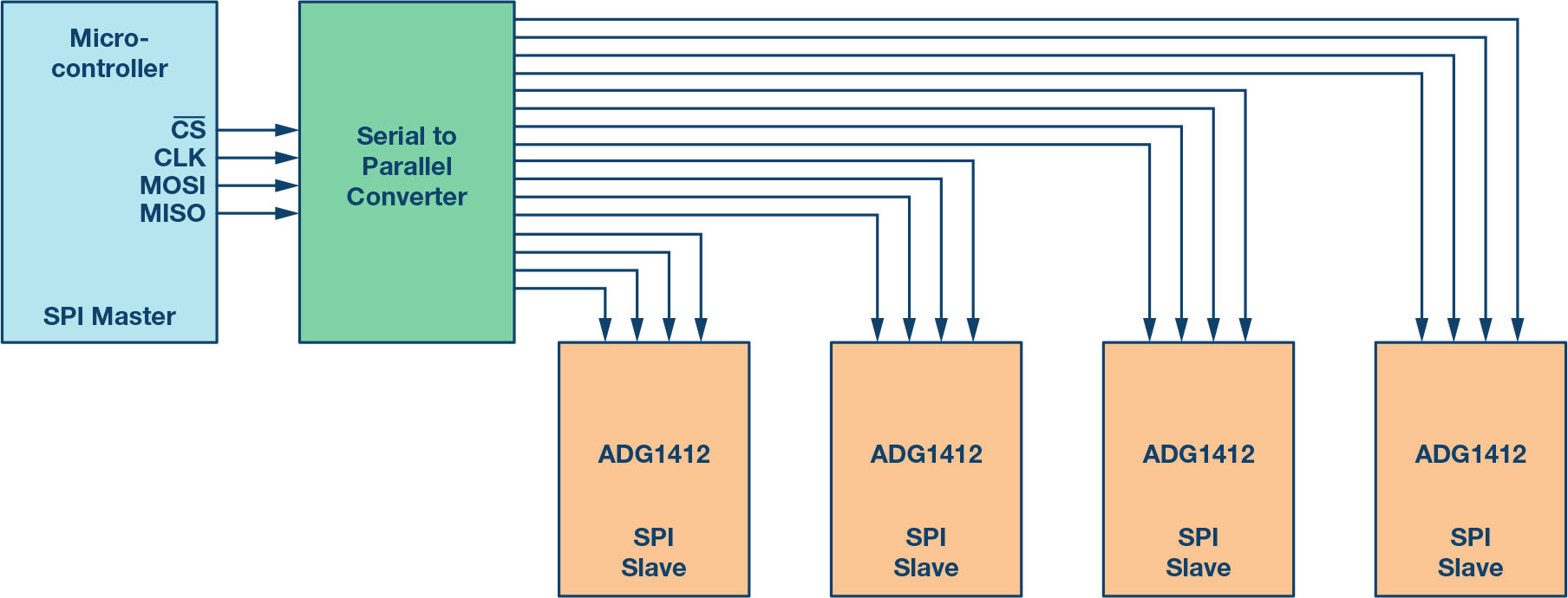
One approach to reduce the number of GPIOs is to use a serial-to-parallel converter, as shown in Figure 11. This device outputs parallel signals that can be connected to the switch control inputs and the device can be configured by serial interface SPI. The drawback of this method is an increase in the bill of material by introducing an additional component.
An alternative method is to use SPI controlled switches. This method provides the benefit of reducing the number of GPIOs required and also eliminates the overhead of additional serial-to-parallel converter. As shown in Figure 12, instead of 16 microcontroller GPIOS, only seven microcontroller GPIOs are needed to provide the SPI signals to the four ADGS1412s.

The switches can be configured in daisy-chain configuration to further optimize the GPIO count. In daisy-chain configuration, irrespective of the number of switches used in the system, only four GPIOs are used from the master (microcontroller).
Figure 13 is for illustration purposes. The ADGS1412 data sheet recommends a pull-up resistor on the SDO pin (Please refer to the ADGS1412 data sheet for further details on daisy-chain mode.).

For the sake of simplicity, four switches have been used in this example. As the number of switches increase in a system, the benefits of board simplicity and space saving is significant. The ADI SPI enabled switches provide a 20 percent overall board space reduction in a 4 × 8 crosspoint configuration with eight quad SPST switches on a 6-layer board.
The article “Precision SPI Switch Configuration Increases Channel Density” provides detail on how precision SPI switch configuration increases channel density.
References:
- ADuCM3029 data sheet. Analog Devices, Inc., March 2017.
- Nugent, Stephen. “Precision SPI Switch Configuration Increases Channel Density.” Analog Dialogue, May 2017.
- Usach, Miguel. AN-1248 Application Note: SPI Interface. Analog Devices, Inc., September 2015.
Piyu Dhaker [[email protected]] is an applications engineer in the North America Central Applications Group of Analog Devices. She graduated from San Jose State University in 2007 with a master’s degree in electrical engineering. Piyu joined the North America Central Applications Group in June 2017. She also previously worked in the Automotive Power Train Group and Power Management Group within ADI.


