
An ADC for the digital world
July 09, 2018
Blog

Microchip?s digitally enhanced high-speed ADC for low-power wireless applications
Today’s digital radio architectures rely heavily upon advanced digital signal processing technology, such as Digital Down-Conversion (DDC) for In-phase and Quadrature (I/Q) signal detection and digital decimation filtering for improving Signal-to-Noise Ratio (SNR). DDC and many other digital processing functions are usually implemented by digital building blocks that require extensive firmware operations using Field Programmable Gate Arrays (FPGAs). Figure 1 shows an example of a software-defined radio receiver employing a super-heterodyne, dual-stage conversion architecture, which is very common in RF communication systems and high-speed data acquisition systems.
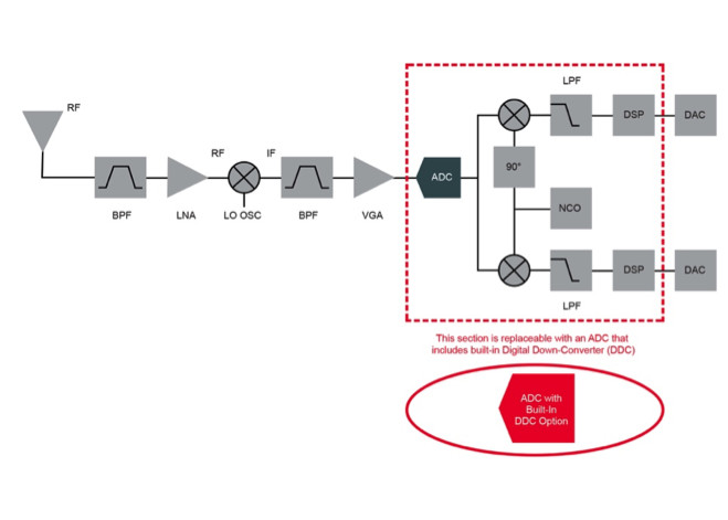
Firmware development for Digital Signal Processing (DSP) building blocks is a very time-consuming task for most system developers. An FPGA also tends to be the highest-cost component in many systems. In order to reduce overall system hardware requirements, complexity, development time and costs, digitally enhanced Analog-to-Digital Converters (ADCs) with built-in Digital Signal Post-Processing (DSPP) options are an excellent solution. These ADCs can handle DDC and many other functionalities without requiring any extra digital processing blocks.
As shown in Figure 1, the conventional ADC and DDC block can be replaced with a digitally enhanced ADC, which can output I/Q signals or up-converted real signals.
The MCP37D31-200 is a digitally enhanced, 16-bit, low-power, 8 channel MUX, 200 Msps ADC with SPI Serial Interface that is capable of performing a variety of DSPP functionalities. It eliminates the need for separate devices or extensive FPGA-based logic in low-power, wireless applications.
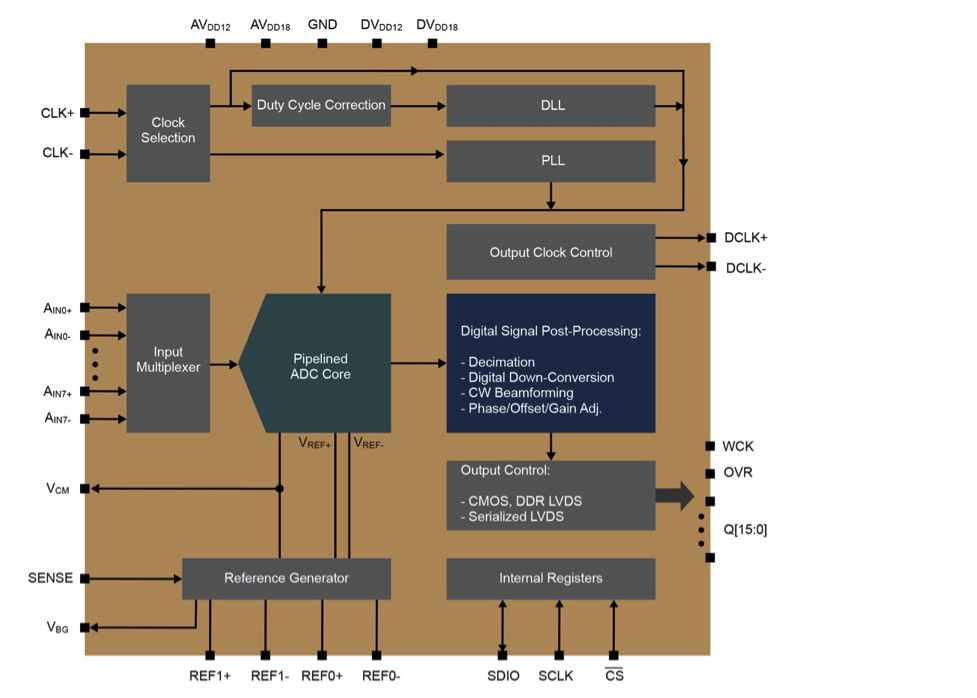
The MCP37D31-200 also features built-in decimation filters for improving SNR, Fractional Delay Recovery (FDR), phase/offset and gain adjust of individual channels, and DDC. In addition, it offers built-in ADC linearity calibration algorithms such as Harmonic Distortion Correction (HDC), DAC Noise Cancellation (DNC) and Dynamic Element Matching (DEM). Available in 12-, 14- and 16-bit versions, this ultra-fast pipelined ADC also delivers some of the lowest-power operation in the industry. Its power dissipation at 200 Msps is 436 mW with CMOS digital I/O, 490 mW with LVDS digital I/O and 390 mW without digital I/O.
This device is well suited for a variety of applications including low-power portable instruments, cellular base stations, ultrasound and sonar imaging and more. If you would like to simplify the development of your low-power wireless application, visit the MCP37D31-200 product page to download the data sheet, learn about design resources and purchase this device.
Want more articles like this? Subscribe to MicroSolutions, Microchip’s bi-monthly digital magazine.


