
Why your Embedded ADC does not Perform to the Data Sheet and how to Improve its Performance, Part 3: PCB Considerations for Addressing Noise
November 19, 2018
Story

This third installment of the series discusses the implementation of a design to meet the expected performance and introduces schematic and layout concepts to address noise.
The first two installments of this series focused on the configurability of an embedded analog-to-digital converter (ADC) and how it’s not possible to maintain ADC performance across all use cases. Once you understand this, you can set the appropriate expectations and move on to implementing a design.
This third installment of the series discusses the implementation of a design to meet the expected performance and introduces schematic and layout concepts to address noise.
Supply decoupling
Providing a stable voltage supply and reference for the ADC is an important factor in circuit design. For a supply distributed across a printed circuit board (PCB), this means providing low impedance paths between the microcontroller (MCU) and other integrated circuit (IC) supply and ground pins, as well as providing low impedance between the supply and ground. This low impedance is an inverse relationship, with frequency seen in capacitance and the impedance, Z, inversely proportional to the frequency. In contrast, more inductive paths will be high impedance because the impedance is directly proportional to the frequency.
The most common way to provide low impedance paths is with power planes and decoupling capacitors. However, the effectiveness of these methods are often compromised because of poor layout choices and component placement. The most classic example is the use of thin and long traces (which are more inductive than capacitive) to connect decoupling capacitors or vias (to power planes) to supply and ground device pins. Congested ball-grid array package types can make avoiding long and narrow traces more challenging, but when planning the escape routing, you should prioritize the supply impedance.
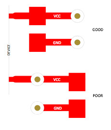
Figure 1 shows another simple but often overlooked mistake in decoupling capacitor placement with respect to both the power plane via and the supply pin. Since the decoupling capacitor is not placed between the supply source and pin, the capacitor’s effectiveness is diminished by the inductance of the additional trace length. [2]
Split analog and digital supplies
While most MCUs have either a single supply rail or recommend connecting the digital and analog supply rails, you can separate the analog and digital supplies (and ground returns) to provide isolation from the rest of the system. A ferrite bead or a short through a 0Ω resistor will often provide enough impedance to separate the supplies. When providing separate analog and digital supplies, keep in mind any requirements regarding the relationships between these two supplies. The voltage difference allowed between the two is often relatively small. Again, a ferrite bead or 0Ω resistor provides enough impedance to separate the supplies, but is small enough to minimize the voltage differences.
ADC reference
Some ADCs use the MCU supply as the reference, which places even more emphasis and care on supply decoupling. Other MCUs provide an internal bandgap circuit to generate references internally; still others provide an interface to supply the reference externally. Generally, an external reference provides the highest quality, but you will still need good layout practices to realize the improved performance.
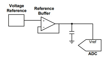
Although it is possible to dedicate a power plane to the reference voltage, this is typically costly and not popular. To minimize the impedance between the reference source and ADC reference input, make the trace width as wide and as short as possible. The placement of the decoupling capacitor, shown in Figure 2, provides a low impedance path to ground and should also follow the same recommendations for the supply decoupling [1].
Signal routing
In addition to providing a clean supply, the signal itself needs to be clean of any unintended signals or interference. Unwanted signals can be the result of conducted or radiated emissions. Since the source of the emissions is not always controllable, let’s look at some simple ways to reduce signal trace susceptibility to interference.
When talking about susceptibility, it can help to identify three components: aggressor, victim and medium. The aggressor is the source of the radiated or conducted interference. The victim, in the context of this discussion, is the ADC input. The medium is the path through which the interference is conducted or radiated. The goal of this signal routing discussion is to address the medium in order to attenuate the amount of energy transmitted from the aggressor to the victim.
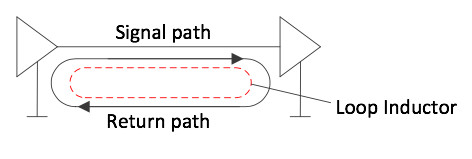
One way to reduce susceptibility is to keep the analog traces between the sensor and the ADC as short as possible. Figure 3 illustrates the inductor loop area created by the signal and return paths. Reducing the signal path will shrink the loop area and reduce the inductance of that loop, making it much less susceptible to fields from aggressor circuits.
Figure 3 also illustrates the importance of ground planes below the signal layer. By supplying a plane directly under the signal path, the return path can follow the path of least impedance (inductance). Splits in the ground plane (or not providing any ground plane) will cause the return current to find an alternate path, which often results in higher impedance and electromagnetic compatibility (EMC) issues.
Another way to make the medium less effective is to make it longer, giving more distance for the signal to attenuate over. This is the main reason for keeping sensitive analog signals away from digital signals such as pulse-width modulators (PWMs) and communication lines (I2C, universal asynchronous receiver transmitter [UART], Serial Peripheral Interface [SPI]). A good rule is to keep these digital signals at least twice the trace width away from the analog signal. You’ll have to break this rule for some designs, and the signals will have to cross paths (on separate layers). In such instances, it’s best to keep the coupling area to a minimum by crossing at 90 degrees, and when possible, insert a ground plane between the signal layers.
Ground planes as well as ground traces (guard traces) are another effective way to attenuate the medium. Ground pours on signal layers (coplanar pours) as well as guard traces can further reduce the impedance from the signal to ground at high frequencies. To ensure that the path to ground is low impedance the guard trace and ground pour widths need to be wide enough to reduce inductance. A good rule is twice the width of the signal trace. Another good practice, with both coplanar ground pours and guard traces, is the use of several vias along the path of the signal. This is referred to as via ‘stitching,’ since the vias are on either side of the signal and resemble a sewing pattern. Using ground planes above and below an internal signal plane can also minimize coupling and shield the sensitive analog trace.
Layout planning
It’s much easier to implement signal routing and use the power planes discussed in the previous sections if you plan for it. Without the important step of planning, developers can easily route themselves into a corner of a PCB, with no way of recovery except to erase and start over.
You should remember two things. The first is the board stackup. Power and ground planes provide low impedance paths and are inherent shields, but adding layers increases board costs. And while cost may be a driving factor, achieving precision measurements will be very difficult without making the necessary investments in the PCB.
The second thing to remember is that separating sensitive analog circuits from noisy digital circuits starts at the MCU. Some manufacturers have intentionally grouped analog-related features to one side of the die or package to help developers keep these signals away from other digital signals on the device. Another MCU feature to help separate analog and digital signals is pin mapping. Pin mapping provides a larger degree of flexibility to customize the digital output location to address both the application and the separation from analog signals.
As a side note, if analog signals pass through a pin mapper – or even if the analog signals are multiplexed with other digital signals – you should confirm that the analog performance is consistent between the dedicated and multiplexed (shared with digital) analog pins. Sometimes, but not always, the protection circuitry around the digital blocks can negatively impact the performance of the analog signal sharing that pin.
With good planning and adherence to good circuit and layout practices, getting data-sheet performance out of the ADC in a custom design is possible. There are some cases in which you cannot remove noise in the circuit design or the PCB layout. These applications lend themselves toward differential signaling, where the noise is treated as common mode and rejected by the ADC. The last and final installment of this series will look at differential signaling and how it addresses noise both inside and outside the design.
This is part three of a series, to read part four, click here.
References
- “Tips and Tricks for Designing with Voltage References.” Texas Instruments e-book SLYC147, 2018.
- “System Design Guidelines for SimpleLink™ MSP432E4 Microcontrollers” Texas Instruments – SLAA770, 2017


