
Ultralow Noise, High Current, Compact DC-to-DC Converter Solution for Signal and Data Processing Circuits
October 05, 2020
Story
One common thread throughout these systems is ever-increasing processing power, resulting in corresponding increases in raw power requirements.
Data processing ICs, such as field programmable gate arrays (FPGAs), systems on a chip (SoCs), and microprocessors, continually increase their reach into telecommunications, networking, industrial, automotive, avionics, and defense systems. One common thread throughout these systems is ever-increasing processing power, resulting in corresponding increases in raw power requirements. Designers are well aware of the thermal management problems of high power processors but may not consider the thermal management issues of power supplies. Not unlike the transistor-packed processors themselves, worst-case thermal problems are inevitable when low core voltages require high current—the overall trend for the power supplies for all data processing systems.
DC-to-DC Converter Requirement Overview: EMI, Conversion Ratio, Size, and Thermal Considerations
Typically, an FPGA/SoC/microprocessor requires a number of power supply rails, including 5 V, 3.3 V, and 1.8 V for peripheral and auxiliary power, 1.2 V and 1.1 V for DDR4 and LPDDR4, and 0.8 V for processing cores. The dc-to-dc converters that produce these rails typically take inputs of 12 V or 5 V, from a battery or intermediate dc bus. To step down these source dc voltages to the much lower voltages required by a processor, switch-mode buck converters are naturally chosen because of their high efficiency at large step-down ratios. Switch-mode converters come in hundreds of flavors, but many can be categorized as either controllers (external MOSFETs) or monolithic regulators (internal MOSFETs).
A traditional switch-mode controller IC drives external MOSFETs and features external feedback control loop compensation components. The resulting converter can be very efficient and versatile, while providing high power, but the number of required discrete components make design relatively complicated and difficult to optimize. External switches can also limit the switching speed, which is a problem when space is at a premium, such as in automotive or avionics environments—as lower switching frequencies result in larger sized components throughout.
Monolithic regulators, on the other hand, can greatly simplify design. This article covers monolithic approaches in depth.
Don’t Overlook the Minimum On- and Off-Times
An important consideration is a converter’s minimum on- and off-times, or its ability to operate at duty cycles sufficient to step down from the input to the output. The larger the step-down ratio, the lower the required minimum on-time (also depending on frequency). In a similar vein, the minimum off-time corresponds to the dropout voltage: how low the input can go before the output is no longer supported. Although increasing switching frequency has the benefit of an overall smaller solution, minimum on- and off-times set the upper limit for operating frequency. In sum, the lower these values, the more leeway you have in designing for small size and high-power density.
Pay Attention to Real EMI Performance
Superior EMI performance is also mandatory for safe operation with other noise sensitive devices. In industrial, telecommunications, or automotive applications, minimizing EMI can be a significant priority for power supply designs. To enable complex systems of electronics to work in concert, without problems arising from overlapping EMI, stringent EMI standards have been adopted, such as the CISPR 25 and CISPR 32 radiated EMI specifications. To meet these requirements, traditional power supply approaches reduce EMI by slowing down switching edges and lowering switching frequency—the former resulting in lower efficiency and higher thermal dissipation, and the latter in lower power density.
Reduced switching frequency also risks violating the 530 kHz to 1.8 MHz AM band EMI requirement in the CISPR 25 standard. Mechanical mitigation techniques can be adopted to reduce noise levels, including complex, bulky EMI filters or metal shielding, but these add significant costs and bulk in board space, component count, and assembly complexity, while further complicating thermal management and testing. None of these strategies meet the requirements of compact size, high efficiency, and low EMI.
Reducing Size While Improving EMI and Thermal Performance, and Efficiency
It is clear that power system design has reached a point of complexity that places significant burdens on system designers. To relieve some of this burden, a good strategy is to look for power supply IC solutions with features that solve many problems at once: reducing the complexity on the board, operating at high efficiency, minimizing heat dissipation, and producing low EMI. Power ICs that can support multiple output channels further simplify design and production.
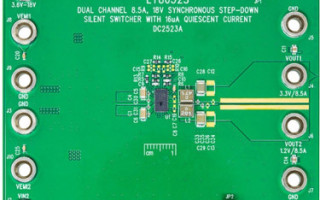
Monolithic power supply ICs, where the switches are incorporated into the package, can achieve many of these goals. For instance, Figure 1 shows a complete dual-output solution board, illustrating the compact simplicity of a monolithic regulator. The integrated MOSFETs and built-in compensation circuitry in the IC used here require only a few external components. The total core size for this solution is only 22 mm × 18 mm, achieved in part by the relatively high, 2 MHz switching frequency.

(Figure 1. Compact, high switching frequency, high efficiency solution with excellent EMI performance.)
The schematic for this board is shown in Figure 2. In this solution, the converter runs at 2 MHz and produces 3.3 V at 8.5 A and 1.2 V at 8.5 A, using two channels of an LT8652S. This circuit can be easily modified to produce output combinations including 3.3 V and 1.8 V, 3.3 V and 1 V, etc. Or, to take advantage of the LT8652S’s wide input range, the LT8652S can be used as the second stage converter, following a 12 V, 5 V, or 3.3 V pre-regulator, to enhance the total efficiency and power density performance. The LT8652S can deliver 8.5 A for each channel at the same time, 17 A for parallel output, and up to 12 A for single-channel operation, due to its high efficiency and great thermal management. With a 3 V to 18 V input range, it can cover most input voltage combinations required for FPGA/SoC/microprocessor applications.

(Figure 2. Dual-output, 2 MHz, 3.3 V/8.5 A and 1.2 V/8.5 A application using two channels of the LT8652S.)
Performance of a Dual-Output, Monolithic Regulator
Figure 3 shows the measured efficiencies for the circuit in Figure 1. For single-channel operation, the solution achieves 94% peak efficiency for a 3.3 V rail and 87% peak efficiency for a 1.2V rail with 12V input voltage. For dual-channel operation, the LT8652S has 90% peak efficiency with 12V input and 86% full load efficiency at 8.5A load current for each channel. Due to the off time skipping function, the LT8652S has an extended duty cycle close to 100%, regulating output voltage with the lowest input voltage range. The 20ns typical minimum on-time even makes it possible to operate the regulator at a high switching frequency, generating a less than 1V output directly from a 12V battery or dc bus—resulting in reduced overall solution size and cost, while avoiding the AM band. Silent Switcher 2 technology with integrated bypass capacitors prevents possible layout or production issues affecting superior benchtop EMI and efficiency performance.

(Figure 3. Efficiency of single and dual output with 2 MHz switching frequency.)
Differential Voltage Sensing for High Current Loads
For high current applications, every linear inch of PCB trace induces significant voltage drop. For the low voltage, high current loads typical in modern core circuitry, which require a very tight voltage range, voltage drops can cause serious issues. The LT8652S features a differential output voltage sensing function, which allows the customer to make a Kelvin connection for output voltage sensing and feedback directly from the output capacitor. It can correct up to ±300 mV of the output ground line potential. Figure 4 shows the LT8652S load regulation for both channels utilizing the differential sensing function.

(Figure 4. LT8652S load regulation with differential sensing function.)
Monitoring Output Current
In some high current applications, output current information must be collected for telemetry and diagnostics purposes. In addition, limiting the maximum output current or derating output current based on operating temperature can prevent damage to the load. Therefore, constant voltage, constant current operation is required to accurately regulate the output current. The LT8652S uses the IMON pins to monitor and reduce the effective regulated current to the load.
While IMON programs the regulated current to the load, IMON can be configured to reduce this regulated current based on the resistance between the IMON and GND. The load/board temperature derating is programmed using a positive temperature coefficient thermistor. When the board/load temperature rises, the IMON voltage rises. To reduce the regulated current, the IMON voltage is compared with an internal 1V reference to adjust duty cycle. The IMON voltage can be lower than 1V, but then it will have no effect. Figure 5 shows the output voltage vs. load current profile before and after IMON current loop is activated.

(Figure 5. LT8652S output voltage vs. current profile.)
Low EMI
For complex electronics systems to work, stringent EMI standards are applied to the individual component solutions. Standards have been widely adopted for consistency across a number of industries, such as the CISPR 32 for industrial and CISPR 25 for automotive. For superior EMI performance, the LT8652S incorporates leading-edge Silent Switcher 2 technology with EMI cancelling design and integrated hot loop caps that minimize noisy antenna size. Coupled with the integrated MOSFETs and small solution size, an LT8652S solution can provide exceptional EMI performance. Figure 6 shows EMI test results for the LT8652S standard demo board shown in Figure 1. Figure 6a shows CISPR 25 radiated EMI with peak detector, and Figure 6b shows the CISPR 32 radiated EMI result.

(Figure 6. Radiated EMI test results of the Figure 1 application circuit. VIN = 14 V, VOUT1 = 3.3 V/8.5 A, VOUT2 = 1.2 V/8.5 A.)
Parallel Operation for Higher Currents and Better Thermal Performance
As data processing speeds soar and the volume of data multiplies, the power of FPGAs and SoCs expands to meet these needs. Power needs power, with supplies expected to keep up in power density and performance. Nevertheless, the merits of simplicity and robustness should not be lost in the quest for increased power density. For processor systems that demand more than 17 A current capability, multiple LT8652Ss can be paralleled, mutually running out-of-phase.
Figure 7 shows two converters connected in parallel to provide 34A output current at 1V. The clock from the master unit is synced to the slave unit by tying the CLKOUT of U1 to the SYNC of U2. The resulting per channel 90° phase difference reduces the input current ripple and spreads the thermal load over the board.
To ensure better current sharing in steady state and during startup, VC, FB, SNSGND, and SS are tied together. A Kelvin connection is recommended for accurate feedback and noise immunity. Place as many thermal vias as possible at the vicinity of the ground pins to the bottom layer to improve the thermal performance. Ceramic caps of the input hot loops should be placed close to the VIN pins.
Load transient requirements imposed by automotive SoCs can be difficult to meet as driving conditions can change drastically, frequently, and quickly, where the SoC must adapt to fast-changing loads without delay. It is not uncommon to see a load current slew rate at 100 A/μs for peripheral power supplies and even higher for core supplies. Yet the voltage transients at the output of the power supplies must be minimized under fast load current slew rates. A fast switching frequency, >2 MHz, enables fast transient recovery, with minimal output voltage excursions. Figure 7 shows the proper loop compensation component values that take advantage of a fast switching frequency and stable dynamic loop response. It is also critical in board layout to minimize trace inductance from the output capacitors of the circuit to the load.

(Figure 7. A 4-phase, 1 V/34 A, 2 MHz solution for an SoC application.)

(Figure 8. Load transient response of the Figure 7 circuit.)
Conclusion
The processing power of FPGAs, SoCs, and microprocessors continually increases, resulting in corresponding increases in raw power requirements. As the number of required power rails and their carrying capacity increases, it is imperative to think small and fast with regard to design and performance of the power system. The LT8652S is a current-mode, 8.5 A, 18 V synchronous Silent Switcher 2 buck regulator, which operates from an input voltage range of 3 V to 18 V, suitable for applications with input sources ranging from a single-cell Li-Ion battery to automotive inputs.
The LT8652S has an operating frequency range of 300 kHz to 3 MHz, enabling designers to minimize external component sizes and avoid critical frequency bands, such as AM radio. Silent Switcher 2 technology guarantees excellent EMI performance without sacrificing the switching frequency and power density nor the switching speed and efficiency. Silent Switcher 2 technology also integrates all necessary bypass capacitors into the package, minimizing the chance of layout or production induced EMI surprises—simplifying design and manufacturing.
Burst Mode operation reduces quiescent current to only 16 μA while keeping output voltage ripple low. The combination of a 4 mm × 7 mm LQFN package and very few external components ensures a very compact footprint while minimizing solution cost. The LT8652S’s 24 mΩ/8 mΩ switches deliver efficiencies of over 90%, while programmable undervoltage lockout (UVLO) optimizes system performance. Remote differential sensing of output voltage maintains high accuracy over the whole load range while being immune to trace impedance, minimizing the possibility of load damage caused by external variety. Other features include internal/external compensation, soft start, frequency foldback, and thermal shutdown protection.
About the Author
Dong Wang is an applications engineer for power products at Analog Devices who began his career at Linear Technology in 2013. He currently provides applications support for nonisolated monolithic step-down converters. Dong Wang has broad interests in power management solutions and analog circuits, including high frequency power conversion, distributed power systems, power factor correction techniques, low voltage/high current conversion techniques, high frequency magnetic integration, and modeling and control of converters. Dong Wang graduated from Zhejiang University in Hangzhou, China, with a Ph.D. in electrical engineering. He can be reached at [email protected].


