
TIA Fundamentals: The Noise Transfer Function Part 4
March 18, 2020
Blog
In Part 4, we?ll dive into the derivation of the noise gain transfer function.
The AC transimpedance amplifier discussion, in my previous blog, TIA Fundamentals: The Parasitics Part 3, provides an understanding of the circuit’s noise gain and stability. In Part 4, we’ll dive into the derivation of the noise gain transfer function.
TIA’s Noise Gain
Let’s start by adding an amplifier noise source, Vn, to the transimpedance amplifier’s total picture. The elements shown in the transimpedance amplifier circuit diagram (Figure 1) provide us with an evaluation of the critical frequency components. For the stability analysis, the input signal source is the noise voltage, Vn. The model of the amplifier’s noise source (Vn) is placed across the amplifier inputs.
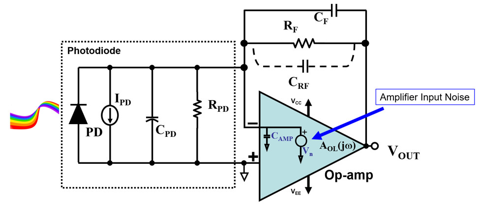
Figure 1. A complete circuit diagram of the transimpedance amplifier includes parasitic capacitors, resistors, and amplifier noise source (Vn).
Putting It All Together
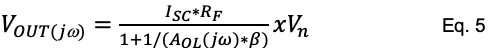
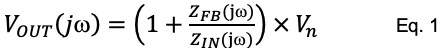
An evaluation of the noise gain response in any amplifier circuit should include a look at the gain of a signal on the amplifier’s noninverting input to the amplifier’s output pin. The complete transimpedance circuit’s noise gain transfer function is:
where:
AOL(jw) is the open-loop gain of the amplifier over frequency.
β is the system feedback factor that equals 1/(1 + ZIN / ZF).
Determining the 1/β Transfer Function
If you assume the amplifier’s open-loop gain AOL(jw) is infinite, the amplifier’s noise-gain transfer function in Figure 1 equals Equation 1:
Where (s) à (jw)
ZFB(jw) is the complex feedback impedance
ZIN(jw) is the complex input impedance
This simplification renders the 1/β first-level transfer function calculations where:
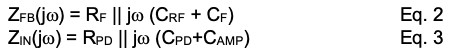
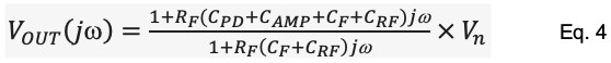
It is very convenient that the feedback elements are combined with ZFB(s) and the input elements are combined with ZIN(s). Let’s pull this together into a form where we can identify the poles and zeroes in the TIA circuit.
To reduce this noise gain equation (Equation 1) into a pole and zero format, our transfer function is now Bode plot-ready with one pole and one zero (Equation 4).
The Bode TIA Noise Plot
A good tool for determining stability is a Bode plot. At this point, let’s discuss some basic analog design guidelines. Classroom instructors will tell you that stable phase margins are greater than 0°. Not true. Out in the field, you are better off designing with a phase margin of 45° or higher. If you drive a step signal into a circuit on a PCB, with a positive phase margin close to 0°, you will have a circuit that will oscillate out of control. This instability comes from unexpected, component parasitics, or uncharacterized capacitances in the PCB layout. The same step signal into an analog circuit with a 45° phase margin will produce approximately 30% overshoot above the input step signal. You will also produce a damped signal that will eventually settle down.
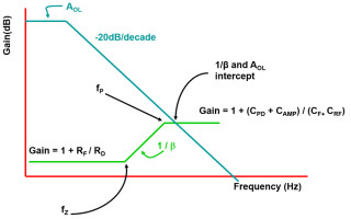
The appropriate Bode plot for this design includes the amplifier’s open-loop gain and the 1/β curve. System elements that determine the noise gain (1/β) frequency response are the photodiode parasitics and the operational amplifier’s input capacitance (ZIN) as well as the elements in the amplifier’s feedback loop (RF, CRF, and CF) (Figure 2).
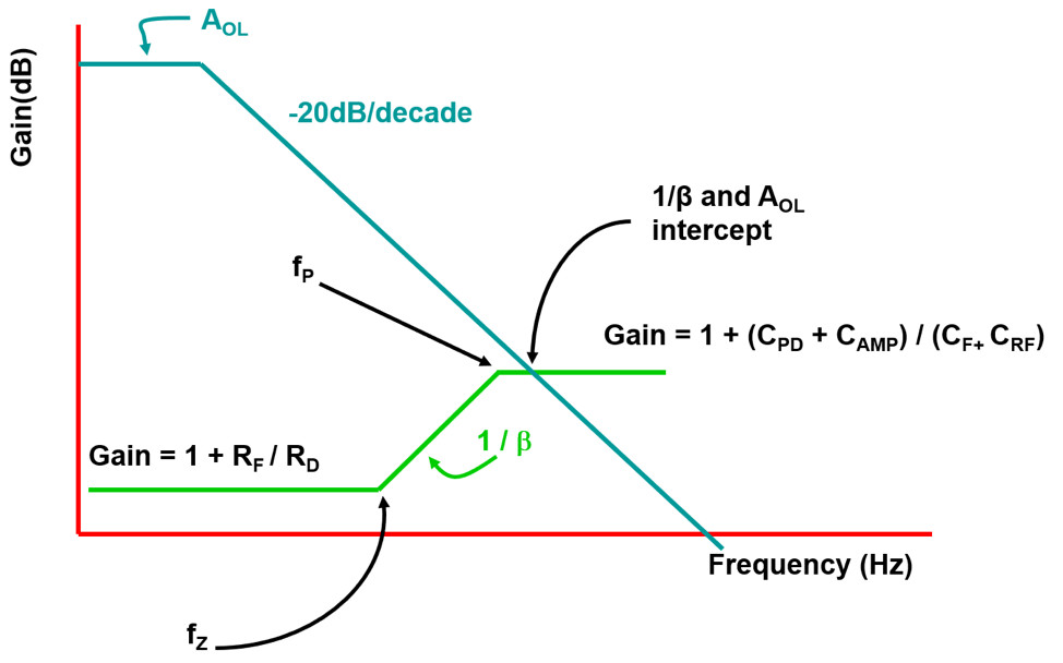
Figure 2. The closure rate between the closed-loop gain (1/β) and the amplifier’s open-loop gain (AOL) is 20dB/decade.
There are important 1/β curve gain values and frequencies to pay attention to in Figure 2. The 1/β curve DC value is equal to 1 + RF/ RD. In this ratio, RF is the TIA’s feedback resistor, usually in the range of 10kW to 10MW.
On the other hand, RD is the photodiode parasitic resistance. This parasitic resistance represents the zero-bias p-n photodiode junction. The materials for photodiodes (and their optic range) are silicon (190nm - 1100nm), germanium (400nm -1700nm), indium gallium arsenide (800nm - 2600nm), lead sulfide (<1000nm - 3500nm), or mercury cadmium telluride (400nm - 14000nm). The photodiode ranges of parasitic shunt resistance are from tens to thousands of megaohms.
Putting these two resistors together, RF/RD, usually equals near zero, making the TIA DC gain equal to 1V/V.
The second important 1/β gain is when the curve becomes flat again at higher frequencies. The gain in this region equals (1 + (CPD +CAMP)/(CF + CRF)). Notice that the high-frequency gain has the summation of the input capacitors in the numerator and the summation of the output capacitors in the denominator.
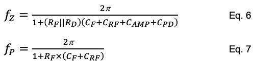
The third important 1/β gain curve’s characteristic are the frequency corners, fZ and fP. The following formulas for the corner frequencies (fZ, Equation 6) and pole (fP, Equation 7) are:
The final interesting part of the Figure 2 graph is where the 1/β curve intersects the AOL(jw) curve. The closure rate between the two curves generally suggests the value of the TIA circuit’s phase margin.
The TIA circuit is stable if the closure rate between these two curves is 20dB, meaning the phase margin is greater than 45°. If the 1/β curve intersects the AOL curve at the pole frequency (fP), the circuit phase margin is 45°. The circuit is not stable if the closure rate is greater than 20dB. This creates a phase margin less than 45°. Once you have the general phase margin, you can estimate if the circuit is stable or not.
There are three ways to correct circuit instability: 1) increase the feedback capacitor, CF, value; 2) change the amplifier to have a higher unity-gain bandwidth; 3) use a different photo detector with a different input capacitance.
But let’s cut to an easy solution for the discussion above. Equation 8 shows a conservative calculation that emulates a Butterworth response with a 65o phase margin and a 5% step response overshoot.
CF = 2* p ((CPD + CAMP) /(2 p RF fGBW)) - CRF Eq. 8
where fGBW is the gain-bandwidth product of the unity-gain stable amplifier
Equation 8 allows you to vary not only the amplifier bandwidth/input capacitance but the the feedback resistor value as well.
Conclusion
In this blog, we’ve shown a way to complete a TIA design, and have shown a clear way to select the TIA’s feedback capacitor (CF). As you are guessing from Equation 8, there are two variables that require further definition àRF, fGBW. Join us for part 5, where we’ll become familiar with the photodiode and learn how your application can help define the photodiode output range, and hence determine the feedback resistor’s value and amplifier selection.


