
Selecting the Optimal Flash Device for your Embedded Application
December 11, 2018
Story

Recent advancements in protocols and memory design enable running the firmware directly out of an off-chip non-volatile memory (NVM) device in an eXecute-in-Place (XiP) fashion.
Most of today’s embedded systems rely on on-chip flash or SRAM for the program memory (firmware). However, these memories are typically expensive in terms of cost and power consumption and also limit the program size to the amount of memory that is implemented on-chip. Recent advancements in protocols and memory design enable running the firmware directly out of an off-chip non-volatile memory (NVM) device in an eXecute-in-Place (XiP) fashion – a method that can potentially mitigate the above-mentioned challenges.
This article will cover advantages and disadvantages of the traditional solutions for embedding the firmware. It will follow with an in-depth discussion of XiP solutions and conclude with recommendations on how to select an optimal XiP architecture.
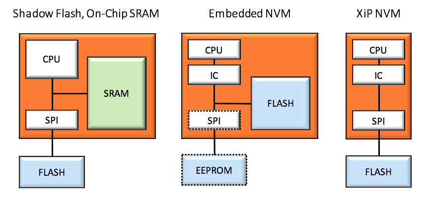
Embedded flash has long been a mainstay of microcontrollers (MCUs). These MCUs augment the on-chip volatile memory arrays with one or more NVM array that stores the firmware and other constants. Achieving this requires a basic CMOS process to be augmented with NVM cells via a large number of extra manufacturing steps. In the past, the cost of adding these manufacturing steps was small, but with advancements in CMOS technology, it becomes more and more complex and expensive to turn a standard CMOS process into one that supports NVM. In fact, while the most advanced CMOS process in mass production today is below 10nm, CMOS with embedded flash lags multiple generations behind at 40nm.
The result is that while MCU vendors could have built products using a process technology that is faster, less expensive and requires lower power, the use of embedded NVM keeps them from doing so. Even when they select an older generation that optionally supports embedded NVM, the price gap between a process that supports flash and one that does not could be over 40 percent. In addition, committing a specific NVM size into the MCU may work well for one application but could be the wrong capacity for another application.
Regardless of all these challenges, embedded NVM will be the mainstay of MCUs for a long time. For smaller designs that can be implemented in a less advanced CMOS process, the use of embedded flash will be the most efficient solution. But higher-performance, lower-power MCUs need alternative solutions.
An alternative approach to using embedded flash is an on-chip SRAM array backed up by an external serial flash device. Upon start-up, the contents of the external flash are copied to the on-chip SRAM and then the MCU starts executing from the SRAM. The big advantage of this solution is the fact that SRAM can be manufactured at the most advanced CMOS processes with no need for process modifications. However, this solution requires two copies of the firmware – one in the external flash and another in the SRAM. Large on-chip SRAM arrays are quite expensive even in advanced process nodes. And, since SRAMs leak current, they need to be turned off when the system is in power-down mode, requiring a repeat of the power-hungry, time-consuming copy operation each time the MCU wakes up. Lastly, as in the case of embedded flash, the size of the SRAM in a specific MCU is fixed and it may be too big or too small for the needs of a specific application.
MCU vendors are looking at new memory architectures to meet the performance and power requirements of emerging intelligent IoT edge devices. The use of XiP is emerging as a preferred solution for higher-performance, lower-power systems. With XiP, the MCU can be implemented in a standard CMOS process technology while only the external flash array needs the special NVM process. The MCU is augmented with an instruction cache that holds the frequently used code segments. Whenever the processor cannot find the required instructions in the cache (cache miss), the MCU initiates an access to the external flash to bring the missing instructions and stores them in the cache. With the introduction of the new JEDEC xSPI protocol (JESD 251), the interface to the flash can may be up to 200MHz with an 8-bit wide data path switching in a Dual-Data-Rate (DDR).
Recently both NXP and ST introduced MCUs that can use external flash for eXecute-in-Place (XiP) operation. ST’s STM32L4+ and the STM32L5 are mid-range MCUs based on Arm Cortex-M4 and M33 cores respectively, while the high-end NXP i.MX RT1050 and other members of the RT10xx family implement a 600MHZ dual-issue Cortex-M7 with 32KB instruction-cache. NXP also supports XiP through its mid-range M4-based Kinetis K8x products and the recently introduced the RT600, an MCU based on the Arm Cortex-M33. The ST MCUs and the Kinetis K8x implement a combination of on-chip flash and support for XiP. The RT600 and the RT10xx products are designed without an on-chip flash, enabling them to achieve very aggressive price points.
When selecting an external flash memory device for eXecute-in-Place, the first questions to be asked are which parts of the firmware will run in XiP mode. Some designers choose a hybrid approach where they keep the performance-critical parts of their program on chip (in ROM, flash or SRAM) and use an external flash in an XiP mode for expanding their system.
Questions regarding this:
- Will all or part of the program be executed from, on-chip ROM, flash or SRAM? If yes, which of these memory types?
- Will all or part of the program be executed directly out of an external flash in XiP fashion?
If the answer to (a) is SRAM, there will be a need for flash outside the SoC for loading the program upon boot. Designers can select an Adesto Phoenix (standard flash), Fusion (flash optimized for battery operation) or EcoXiP (Octal flash optimized for XiP). Phoenix should be selected for applications that are cost sensitive and where the throughput is not critical. Fusion would fit the best applications that have very tight power constraints. Adesto’s EcoXiP should be considered in this case only if the customer also needs high-performance in XiP mode or needs the throughput of an Octal flash device for very fast boot or frequent data-read operations – as is the case for artificial intelligence inference engines.
Assuming that the answer to (b) was positive (at least part of the firmware needs XiP), the next issue is to figure out how much performance is required. EcoXiP delivers about 4X the throughput of a standard flash device as a result of the high speed Octal DDR interface. In addition, the wrap-and-continue command improves the achievable throughput even more. There are a number of questions to ask:
- Will the SoC include an instruction cache? (without an instruction cache, the XiP performance will be very low; however the advantage of EcoXiP over Quad devices will be more significant)
- What frequency will the CPU run at and what’s the frequency of the SPI bus?
- What level of performance is required while running in XiP?
- Will the device need field software updates (typically referred to as Over-The-Air (OTA) updates)?
The answer to (c) is crucial. At low frequency and with a low demand for XiP performance, it is quite feasible to execute directly out of a standard Quad SPI flash device. However, even with a very small percent of misses in the instruction cache, executing out of a Quad device will deliver about 50 percent of the CPU performance when compared with running out of EcoXiP.
Note that if the response to (d) is positive, the read-while-write capability of EcoXiP will make OTA updates much easier if the SoC is built without other code storage memories (relying on XiP only). There are other solutions for OTA updates without having read-while-write but they are all SRAM intensive and require complex firmware.
For more information about the difference in XiP performance between Quad and Octal devices, please refer to the article ‘Is your Quad Device Choking your System Performance?’


