
Maximize the Performance of Your Sigma-Delta ADC Driver
September 24, 2020
Blog

Have you ever checked how many entries are in the web for 'design buffer for an ADC'? It can be hard to find what you are looking for among more than 4 million references.
Have you ever checked how many entries are in the web for “design buffer for an ADC”? It can be hard to find what you are looking for among more than 4 million references. Probably not a big surprise to most analog and mixed-signal data acquisition system design engineers as designing the external front end for an unbuffered analog-to-digital converter (ADC) requires a lot of patience and advice. It is often seen as an art form, the preserve of eccentric gurus who have mastered their craft over many years. To the uninitiated, it is a frustrating task of trial and error. Most of the time the frustration becomes an annoying companion due to the number of interrelated specifications, which forces many trade-offs (and evaluations) until the optimum results are achieved.
The Challenge
The design of the amplifier stage consists of two different stages related between them, so the problem becomes difficult to model mathematically, especially due to the nonlinearity associated with both stages. The first step is to select the amplifier that will buffer the sensor output and drive the ADC inputs. The second step is to design a low-pass filter to reduce the input bandwidth, which minimizes the out-of-band noise.
The ideal amplifier provides just enough bandwidth to correctly buffer the signal generated by the sensor or transducer, without adding extra noise, and providing zero power consumption, but the ideal is far away from the real amplifier. In most cases, the amplifier specifications are going to define the overall system performance, especially in terms of noise, distortion, and power. To get a better picture about the problem, the first step is to understand how a discrete time ADC operates.
A discrete time ADC gets a sample of a continuous time analog signal that is later converted into a digital code. When the signal is sampled, depending on the type of analog converter, there are two different scenarios with same inherent problem.
SAR ADCs integrate a sample-and-hold, also known as track-and-hold, which is fundamentally a switch and a capacitor that freeze the analog signal until the conversion is done, as shown in Figure 1.

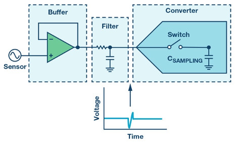
Discrete time Σ-Δ ADCs, or oversampling converters, implement a similar input stage, that is, an input switch with some internal capacitance. In the case of Σ-Δ ADCs, the sampling mechanism is slightly different, but a similar input architecture of sampling occurs where switches and capacitors are used to hold a copy of the analog input signal.
In both cases the switch is implemented in a CMOS process with a non-zero value of resistance when closed, typically a few ohms. The combination of this series resistance with the sampling capacitor, in the range of pF, means that the ADC input bandwidth is often very large, and it is in many cases much larger than the ADC sampling frequency.
The Bandwidth Problem
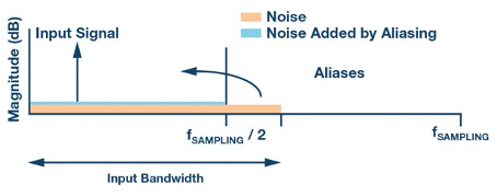
The input signal bandwidth is a problem for the converter. In sampling theory, we know that frequencies above the Nyquist frequency (half of the ADC sampling frequency) should be removed, otherwise those frequencies are going to generate images, or alias, into the band of interest. Noise, typically, has a spectrum where a significant amount of power can exist in the frequency band above the Nyquist frequency of the ADC. Unless we deal with this noise, it will alias down below the Nyquist frequency and add to the noise floor, as shown in Figure 2, effectively reducing the dynamic range of the system.
The ADC input signal bandwidth and, by extension, the buffer output bandwidth represent the first problem to be solved. To ensure that the noise does not get aliased down, the bandwidth of the ADC input signal must be limited. This is not a trivial problem.
Typically, the amplifier is chosen based on the specification for a large signal bandwidth—that is, slew rate—and gain bandwidth product to cover the worst case condition for our input signal, which defines the faster event our ADC can track.
However, the effective noise bandwidth of the amplifier is equivalent to the small signal bandwidth (typically considered for signals less than 10 mV p-p), and this is often at least four to five times higher than the large signal bandwidth.
In other words, if our large signal specifications are selected for 500 kHz, the small signal bandwidth could easily be 2 MHz or 3 MHz, potentially allowing a lot of noise sampled by the ADC. Consequently, the small signal bandwidth should be limited externally before feeding the analog signal into the ADC or the noise measured is going to be three to four times the ADC data sheet specifications, which is not good.

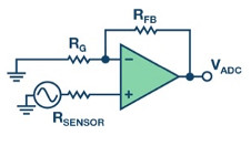
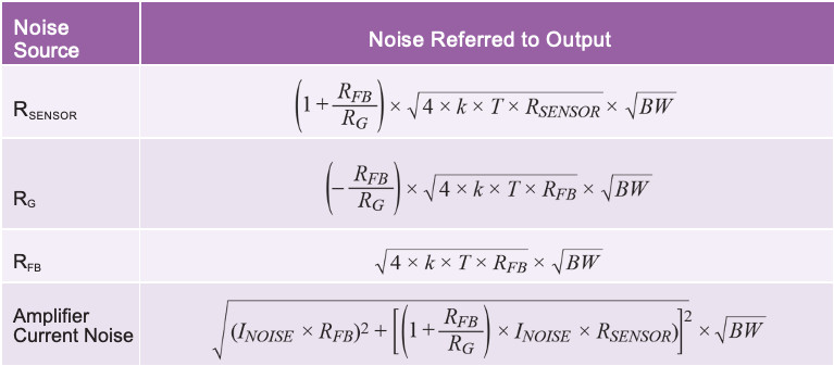
 T is the temperature in Kelvin. Remember that the thermal noise generated by the amplifier depends on the amplifier gain, and the total system bandwidth. An example for the circuit is shown in Figure 3 and the noise sources are summarized in Table 1, where:
k is Boltzmann’s constant (1.38 × 10⁻²³ J/K), resistor values are expressed in Ω, and BW refers to small signal bandwidth.
Previous equations make clear the importance of adding a low-pass filter with enough attenuation before the ADC input pin to minimize the noise sampled, as the noise is proportional to the square root of the bandwidth. Typically, a first-order low-pass filter implemented with a discrete resistor and capacitor, with a low enough cut-off frequency eliminates much of the wideband noise. A first-order low-pass filter has the added benefit of reducing the amplitude of any other larger signals outside of the band of interest before they are sampled, and potentially aliased, by the ADC.
However, this is not the whole story. The internal ADC switch resistance and the capacitor defines the analog input bandwidth, but also creates a time-domain charge-discharge cycle due to the varying input signals. Each time the switch (the external circuitry connected to the sampling ADC capacitor) is closed, the internal capacitor voltage may be different from the voltage previously stored on the sampling capacitor.
What Is the Kickback Problem?
The classic analog question: “If you have two capacitors in parallel connected with a switch, the switch is open and one capacitor stores some energy, then what happens to both capacitors when the switch is closed?”
The answer depends on the energy stored by the charged capacitor and the ratio between the capacitors. For example, if both capacitors are of the same value, the energy will be shared between them and the voltage measured between capacitor terminals will be halved, as shown in Figure 4.

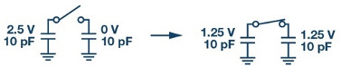
This is the kickback problem.
Some ADCs perform internal calibrations to compensate for internal errors, known as auto-zero calibration. These procedures bring the sampling capacitor to a voltage close to the rails or another voltage, such as the reference voltage divided by two.
This means that the external signal buffered by the amplifier and the sampling capacitor—that must hold the analog value in order to acquire a fresh sample—are very often not at the same potential (voltage). Consequently, the sampling capacitor must be charged or discharged to bring it to the same potential as the buffer output. The energy required in this process will come from the external capacitor (the one from the low-pass RC filter) and the external buffer. This redistribution of charge, and settling of the voltages, will take a finite amount of time during which the voltage seen at the various points in the circuit will be disturbed, as shown in Figure 1. There can often be a significant amount of charge being redistributed, which is equivalent to current flowing to or from the amplifier and into the capacitors.
The consequence is that the amplifier should be able to charge/discharge the external capacitor of the low-pass filter and the sampling capacitor of the ADC in a very limited time, with the current limiter added by the low-pass filter resistor.
Being more specific, the amplifier should be able to charge/discharge the capacitors within a given error, from the sampling capacitor and external sources. The cutoff frequency of the external low-pass filter should be a little bit higher than the band of interest, which is defined by the time constant of the filter, the number of bits of the ADC, and the worst-case transition between samples—that is, the worst input step that we should be able to measure accurately.
How Do We Solve the Kickback Problem?
The easier answer to solve the problem would be to choose an amplifier with enough slew rate, bandwidth gain product, open-loop gain, and CMRR, and place the highest capacitor you may find in the market at the output with a resistor small enough to satisfy low-pass filter bandwidth requirements.
As the capacitor is really big, the kickback problem will be negligible, and the bandwidth is limited by the LP filter, so problem solved, right?
Bad news. The previous solution is not going to work, but if you are curious and try the previous setup, then you will discover two things: the capacitor is going to be the size of a condensed milk container and the amplifier will not like imaginary impedances connected at the output.
The amplifier’s performance is dependent on the imaginary load seen by the amplifier. In this case, the low-pass filter penalization is a degradation on THD and settling time. An increase in settling time would have the effect of leading the amplifier to become unable to charge the capacitors such that the voltage that the ADC sample is the correct final voltage. This would lead to further nonlinearity in the output of the ADC.
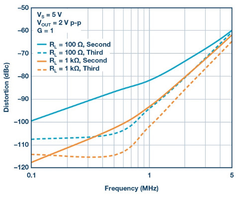
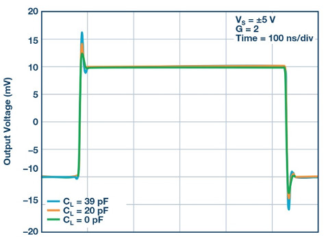
To illustrate the previous statement, Figure 5 shows the performance difference between different amplifier output currents or resistive loads. Figure 6 shows the small signal overshoot due to the capacitive load, which affects settling time and linearity.


To minimize this problem, the amplifier output should be isolated from the external capacitor by the series resistor of the low-pass filter.
The resistor should be high enough to guarantee that the buffer is not going to see the imaginary impedance, but small enough to satisfy the required input system bandwidth and minimize the IR drop across the resistor due to the current flowing from the buffer, which can cause a voltage drop that may not be settled quickly enough by the amplifier. In parallel, the resistor should allow the external capacitor to reduce to a value small enough to minimize the kickback without affecting the settling.
You can find more information here.
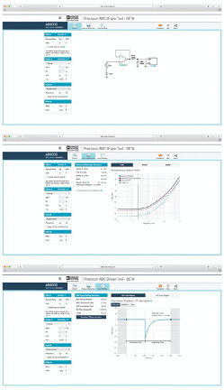
Luckily for us, there are tools that allow us to predict the combined performance of the DAC, the amplifier, and the filter—like the Precision ADC Driver Tool.
The tool can simulate the kickback, as well as noise and distortion performance, as shown in Figure 7.

Rule of Thumb for Low-Pass Filters
Typically, a first-order low-pass filter is seen in many recommendations, but why doesn’t anyone use a higher filter order? Unless your device is going to be used in an application with specific requirements to remove larger out-of-band interferers or harmonics in the input signal, increasing the order of the filter will add an extra layer of complexity to your system. In general, the trade-off is leaving the small signal bandwidth a little bit higher than you need, which will impact the noise at the expense of being able to drive the ADC input stage easily—and reduce power and cost—due to the amplifiers.
Reducing the Burden
We previously mentioned that the amplifier does not like imaginary impedance and/or deliver high currents, and this is an element added by the capacitor that is needed to minimize the kickback problem.
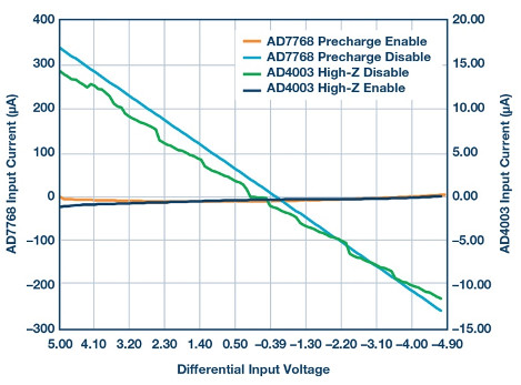
The only way to improve the situation is by reducing the kickback itself. This solution has been adopted by the latest ADI converters, like the AD7768 and the AD4000.
The solutions adopted in each of the devices are different due to different converter architectures. The AD4000 SAR ADC can operate at supplies below the analog input range. The solution adopted is called high-Z mode and is only available for sampling frequencies below 100 kHz.
In the AD7768, the supplies equal or become higher than the analog input range. The solution adopted in the AD7768 is called precharge buffer and, as opposed to the high-Z mode, this operates up to the maximum ADC sampling frequency.
Both solutions are based on the same principle of operation; the main difficulty in driving the ADCs is the capacitive charge redistribution. In other words, the lower the voltage drop seen by the input buffer and the low-pass filter when the internal switch reconnects the sampling capacitor, the lower the voltage kick, which minimizes the ADC input current. Consequently, the easier it is to drive the ADC, the greater the settling time is reduced. The voltage drop across the filter resistance reduces, so the ac performance receives a boost.
The effect on the input current against precharge buffer and high-Z enable and disable can be seen in Figure 8.

The higher the input current, the higher (that is, faster) the amplifier bandwidth should be. Therefore, the higher the input low-pass filter bandwidth should be, and this impacts the noise as well.
For instance, using the SINAD accounts for harmonics as noise performance, for a 1 kHz input signal sampled at 1 MSPS. At different filter cut-off frequencies, we get something like shown in Figure 9.

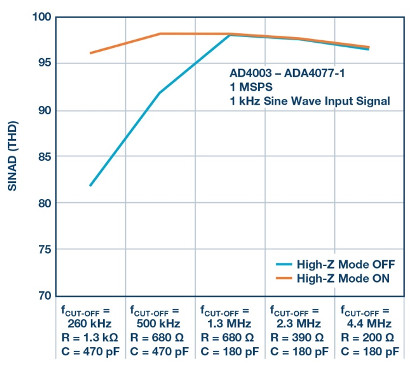
The previous figure shows that low input current (high-Z mode on) reduces the cutoff filter frequency requirements, as well as IR drop in the filter resistance value, boosting the ADC performance, compared with the exact same configuration but high-Z mode off.
In Figure 9, it can be observed that by increasing the input filter cutoff frequency, the external amplifier can charge/discharge the sampling capacitor faster at the expense of higher noise. For instance, with high-Z mode on, the noise sampled at 500 kHz is less than at 1.3 MHz. Consequently, the SINAD is better at 500 kHZ input bandwidth. In addition, the capacitance required by the low-pass filter gets reduced, improving amplifier driver performance.
Circuit Design Benefits
The addition of these easier-to-drive, or burden-reducing, features implemented in ADI’s latest ADCs has some significant impacts on the overall signal chain. The key advantage that the ADC designer has in bringing some of the drive problem into the ADC silicon itself is that the solution can be designed to be as efficient as possible for the signal requirements of that ADC, thereby solving a few problems including input bandwidth and amplifier stability.
The reduction of the current into the ADC input, and therefore reduction of the kickback, means that the amplifier has a lower voltage step to deal with, but still has the same full sampling period as a standard switched-capacitor input.
Having a smaller step voltage to settle (ramp to final value) over a given period is the same as having a longer period to settle a larger step. The net effect is that the amplifier now does not need to have such a wide bandwidth to sufficiently settle the input to the same final value. A reduced bandwidth usually means a lower power amplifier.
Another way to look at this is to imagine how an amplifier that would normally not be expected to have enough bandwidth to settle the input of a given ADC can now achieve enough settling when the precharge buffers are enabled.
The ADI application note AN-1384 shows the performance achievable with a range of amplifiers when paired with the AD7768 in each of its three power modes. One of the amplifiers shown in this document, the ADA4500-2, shows that it struggles to settle the input of the AD7768 in median power mode (THD is >−96 dB) when the precharge buffers are not used. However, when precharge buffers are enabled, the performance improves dramatically to better than −110 dB THD.
Since the ADA4500-2 is a 10 MHz bandwidth amplifier and the bandwidth required to settle the AD7768 in the given mode is approximately 12 MHz, we see that the use of this lower bandwidth amplifier has now been enabled by the easy-to-drive feature. In this way, these features not only enable easier design of the front-end buffer circuit, but also allow more freedom in selecting components to stay within system power or thermal ceilings.
A secondary advantage to having reduced current into the analog input pin of the ADC is that there is now less current flowing through the series resistor that is used as part of the input RC network.
For traditional ADC inputs, the relatively large current meant that only small value resistors could be used, otherwise large voltage drops would be developed across this resistor. A large voltage drop here can lead to gain error or linearity errors in the ADC conversion result.
However, using smaller resistor values also has its challenges. Achieving the same bandwidth of the RC using a smaller resistor means using a larger cap instead. However, this large cap and small resistor combination can lead to instability of the buffer amplifier.
The reduced current, encountered when using the easy-to-drive features, means that larger value resistors can be used without affecting the performance, and ensuring the system’s stability.
Circuit Performance Benefits
Taking what we have already stated as the benefits to the circuit design, it becomes clear that there are also performance benefits, or opportunities to further improve performance, using these features.
The benefit already mentioned, being able to achieve better performance with lower bandwidth amplifiers, can also be employed to extend the performance of more optimal systems. For example, even with a well-settled input signal, there may still be some mismatch between the inputs as that final settling is happening. So, enabling the precharge buffers, f or example, will mean that this final settling is much smaller, so supreme levels of THD can then be achieved where previously this would not have been possible.
The reduction in the current going through the series resistor of the RC network also benefits the performance. Also, not only is the input current significantly reduced, it has almost no dependence on the input voltage. Improved THD can be achieved since any mismatches in the resistors on the input pair will lead to smaller voltage differences seen at the ADC input, as well as the voltage drops not having a signal dependency.
The lower input current also has an effect on offset and gain accuracy. Because of the reduction in absolute current, as well as the reduction in signal dependent current changes, there are less chance that variation in component values across each channel or across each physical board will lead to large variation in offset and gain errors (for the same reason, lower current leads to smaller voltages across series resistances). With pre-charge buffers, better absolute offset and gain error specifications can be achieved, as well as consistent performance across boards or channels within a system.
There is another benefit to the lower current in systems where the ADC sampling rate changes to adapt to different signal acquisition needs, such as in data acquisition cards. Without pre-charge buffers, the voltage drops across the input passive components vary with the sample rate of the ADC, since the ADC input cap will charge and discharge more often at higher sampling rates. This applies to both the analog input path and the reference input path, and this variation in voltage is seen by the ADC as sample rate dependent offset and gain errors.
However, with pre-charge buffers enabled, the absolute current, and therefore the absolute voltage drop, is much smaller to begin with, so the change in voltage as the ADC sample rate changes will also be much lower. In the end system, this means that there is less need to recalibrate the system offset and gain errors as the sample rate is adjusted, and that offset and gain errors are less sensitive to changes in ADC sampling rates.
Cost Benefits
One of the main benefits of the easy to use features is related to the total cost of ownership. The different facets of the design and performance benefits lead to a potentially lower development cost and operational cost.
- Easier design means less design effort and faster time to a first prototype.
- Easier design means greater chance of success the first time in prototype design.
- The easier-to-drive feature may allow lower bandwidth and therefore lower cost amplifiers to be used.
- Offset and gain benefits may allow reduced calibration at factory.
- Performance improvement may allow reduced calibration in field or on-demand, thus leading to reduced downtime and/or improved throughput.
Real Examples Using AD7768-1
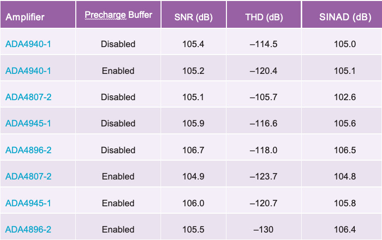
Table 2 shows some measured data from the AN-1384 application note, which helps designers choose the appropriate amplifier to drive the AD7768-1 ADC. The examples in the table show that there are significant possible improvements when the precharge feature is enabled on some amplifiers. The reason for the improvement in THD in particular is due to a combination of the previously mentioned effects of the reduced burden that the ADC places on the drive circuitry. For example, the configuration using the ADA4945-1 amplifier achieves a 4 dB improvement in THD when the precharge buffers are enabled. Similarly, the ADA4807-2 circuit can achieve an increase of 18 dB in THD. What these examples show is that amplifiers that are able to achieve reasonable performance on their own can achieve headline levels of performance when used in conjunction with the easy-to-drive features available in many of ADI’s newest ADCs.
 Designing a circuit to drive an unbuffered ADC is not a trivial thing and requires a proper methodology and trade-off considerations due to the kick-back of the converter and bandwidth requirements. Many times, the required circuitry is going to define the overall system performance in terms of THD, SNR, and power consumption.Conclusion
The latest ADI precision converters for both SAR and Σ-Δ technologies integrate a set of features to minimize the converter input current. This minimizes the kickback, greatly reducing and simplifying the external circuitry, achieving specifications numbers that were not previously possible. This makes the SAR and Σ-Δ technologies easier to use, reduces the engineering time, and improves system specifications.
Stuart Servis [[email protected]] is a product applications engineer at Analog Devices, where he works in the precision signal chains team within the Instrumentation and Precision Technology Group. His area of expertise is precision data acquisition signal chains, based on Σ-Δ and SAR ADCs. He received his B.Sc. in applied physics and electronics from the National University of Ireland in Galway.
Miguel Usach Merino [[email protected]] received his degree in electronic engineering from Universitat de Valencia. Miguel joined ADI in 2008 and works as an applications engineer in the Linear and Pr


