
It's an Exciting Time for Software Developers Who Want to Use FPGAs
June 19, 2020
Story
The vast majority of embedded software developers focus on coding for MPUs and MCUs; relatively few have any experience with regard to using field-programmable gate arrays (FPGAs).
It’s a funny old world when you come to think about it. As you may or may not know, my degree is in Control Engineering (now called System Engineering). The course consisted of a major in math and minors in electronics, mechanics, hydraulics, and fluidics (don’t ask what we did in our spare time).
Although I dabble with regard to writing software, I specialize in creating code fails in strange and wonderous ways. I’m a hardware design engineer by trade. My first position was as a member of a team designing central processing units (CPUs) for mainframe computers.
When MPUs and MCUs first appeared on the scene in the 1970s, the vast majority of folks who wrote software were those working on “big iron” mainframes and minicomputers. As a result, it was predominantly hardware engineers who wrote the original programs for MPU/MCU-based embedded systems.
These days, of course, there’s an ever-increasing industry-wide interest in software coding. In fact, one of the keynote presenters at the Xilinx Developer Forum (XDF) in 2019 noted that the “engineering pie” now comprises of 80% software developers versus only 20% hardware designers. This may suggest I’m a member of a dying breed, but I prefer to believe I’m becoming ever-more special as the years go by. (When I was a young lad, my mother used to tell me I was special, and I foolishly took this to be a compliment. I also remember my father telling me that I was beautiful when I was asleep, and I thoughtlessly took that to be a compliment, also.)
If you have a quick Google while no one is looking, you’ll be presented with estimates that there are around 22 million software developers in the world. Of these, the majority focus on application-level and infrastructure-level coding, leaving only around 1.2 million to focus on embedded systems.
In turn, the vast majority of embedded software developers focus on coding for MPUs and MCUs; relatively few have any experience with regard to using field-programmable gate arrays (FPGAs). This is unfortunate because although regular processors are great for performing decision-making and control chores, they are horribly inefficient when it comes to performing many data processing tasks. By comparison, FPGAs have the ability to perform complex data processing assignments in a massively parallel fashion, thereby allowing them to provide dramatic algorithmic acceleration.
In many cases, the ideal solution is to be found by combining the decision-making and control abilities of regular processors with the algorithmic processing capabilities provided by hardware accelerators implemented in an FPGA’s programmable fabric. In order to facilitate this, Xilinx created the Zynq family of SoC FPGAs, which combine hardened processor cores with programable fabric. The Zynq 7020, for example, provides dual-core 667 MHz 32-bit Arm Cortex-A9 processors (with cache and floating-point units) along with 13,333 slices of programmable logic.
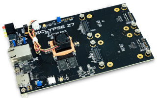
The only problem is how to make the advantages of FPGAs available to software developers who have no time to learn about FPGAs and no interest in doing so. The solution is Digilent’s Eclypse Z7 Development Board with SYZYGY-compatible expansion.
Eclypse Z7 Development Board (Image source: Digilent)
In addition to the aforementioned Zynq 7020, the Eclypse Z7 also boasts 1 GB of DDR3L memory, a MicroSD card slot, and a Gigabit Ethernet interface. Of particular interest to the developers of embedded systems for high-speed instrumentation, medical devices, software defined radio (SDR), and many other applications is the fact that -- along with two Pmod interfaces -- the Eclypse Z7 also provides two Zmod interfaces.
Until recently, anyone who wanted to prototype or develop new FPGA-based systems was limited by the capabilities of the two most commonly used expansion schemes: Pmod and FMC. The Pmod (peripheral module) interface is an open standard that was defined by Digilent and has been widely adopted across the industry. Pmod is ideal for low-speed peripherals in the 1 to 50 MHz range; the 6-, 8-, and 12-pin connectors are inexpensive to implement; and there are many low-cost peripheral modules available off-the-shelf.
At the other end of the spectrum is the ANSI/VITA FMC (FPGA Mezzanine Card) standard, which is more suited to high-performance peripherals with data rates up to 10 Gbps. In this case, the 72-pin and 200-pin connectors are much more expensive, and the peripherals themselves can cost anywhere up to thousands of dollars.
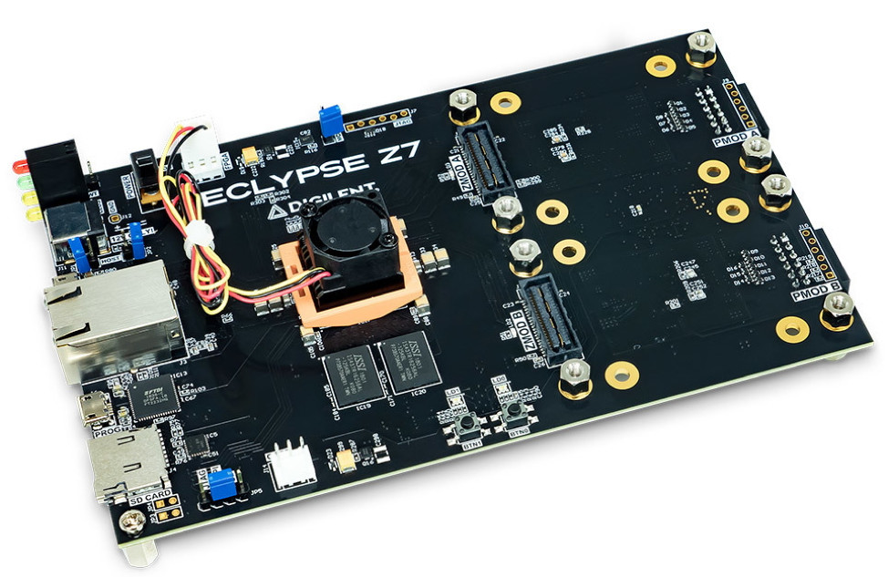
In order to bridge this gap, the folks at Opal Kelly created the SYZYGY (pronounced “Sizz-Uh-Gee”) open standard for connecting high-performance peripherals to FPGA hardware. (See also the SYZYGY Origin Story.) SYZYGY addresses the need for a compact, low cost, low pin-count, high-performance connectivity solution between FPGAs and hardware peripherals required for applications like high-speed data acquisition, digital image capture, software-defined radio, and digital communication.

Eclypse Z7 Development Board with two SYZYGY modules attached (Image source: Digilent)
Currently, two Digilent SYZYGY modules are available: a dual-channel, 14-bit, 100 megasample-per-second (Msps) analog-to-digital converter (ADC), and a corresponding dual-channel 14-bit digital-to-analog converter (DAC). These modules may be purchased independently or bundled with the Eclypse Z7.
But wait, there’s more, because the powerful Eclypse Z7 hardware is supported by an innovative software architecture that allows software developers to dip their toes in the FPGA waters.
In the Zynq-7020 SoC FPGA, the Programming System (PS) portion of the device -- that is, the dual-core 32-bit Arm Cortex-A9 processors -- is connected to the Programmable Logic (PL) portion of the system using high-speed AXI busses. This means that peripheral functions and hardware accelerators implemented in the PL can easily communicate with software running on the PS.
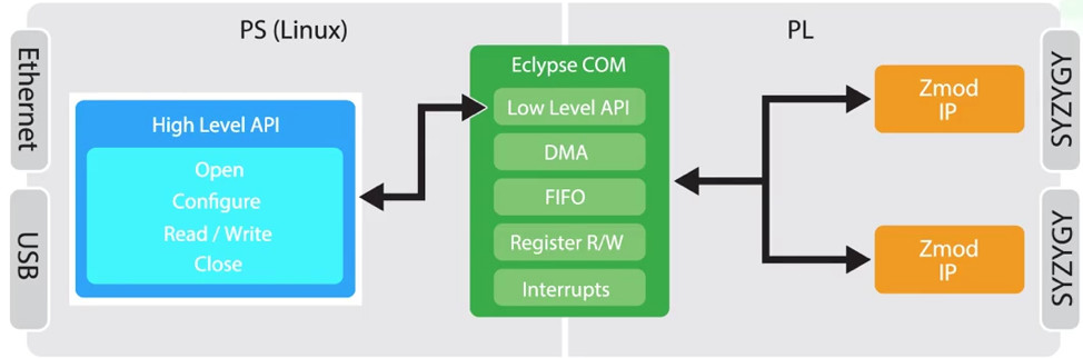
Eclypse Z7 software architecture (Image source: Digilent)
The Eclypse Z7’s software architecture includes pre-built Linux images along with a high-level API that software developers can access using familiar programming languages. This enables the developers to leverage the benefits of FPGA hardware acceleration without the complexity of having to directly interface with the FPGA themselves.
All I can say is that it’s an exciting time for embedded software developers who want to enjoy the advantages offered by FPGAs without actually having to learn anything about FPGAs. Even more exciting is the fact that Digilent are asking us for our suggestions as to which peripheral functions we think they should next implement as Zmod modules.


