Clock Skew in Large Multi-GHz Clock Trees
January 28, 2019
Story

This article identifies several areas of concern in the design process, manufacturing process, and application environment that can cause clock skews of 1 ps or more.
Introduction
It is not uncommon for large clock trees to route clock signals through multiple clock devices, using multiple transmission line types, and across multiple boards and coaxial cables. Even when best practices are followed, any one of these media can introduce greater than 10 ps clock skew. However, in some applications, it is desired for all clock signals to achieve less than 1 ps skew. Some of these applications include phased array, MIMO, radar, electronic warfare (EW), millimeter wave imaging, microwave imaging, instrumentation, and software-defined radio (SDR).
This article identifies several areas of concern in the design process, manufacturing process, and application environment that can cause clock skews of 1 ps or more. With regards to these areas of concern, several recommendations, examples, and rules of thumb will be provided to help the reader gain an intuitive feel for the root cause and magnitude of clock skew errors.
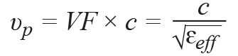
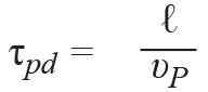
Delay Equations for Transmission Lines
A list of equations is provided that estimate propagation delay (τpd) for a single clock path and delta propagation delays (Δτpd) for multiple clock paths or a change in environmental conditions. In a large clock tree application, Δτpd between clock traces is a portion of the total system’s clock skew. Equation 1 and Equation 2 provide the two main variables that control a transmission line’s τpd: the transmission line’s physical length (?) and effective dielectric constant (?eff). Referring to Equation 1, vp represents the transmission lines phase velocity, VF represent the velocity factor (%), and c represents the speed of light (299,792,458 m/s).
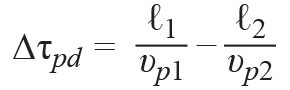
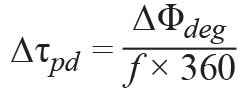
Equation 3 calculates the delta propagation delay (Δτpd) between two transmission lines.
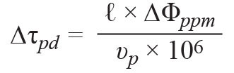
Transmission line dielectric materials have properties that change with temperature. The dielectric constant’s temperature coefficient (TCDk) is often provided in a plot of phase change (Δ?ppm) in parts per million (ppm) vs. temperature, where the Δ?ppm value compares the phase at a desired temperature to the phase at a reference temperature, typically 25°C. For a known temperature, Δ?ppm, and transmission line length, Equation 4 estimates the change in propagation delay from the reference temperature.
Coaxial cable dielectric materials have properties that change based on the bend in a cable. The radius and angle over which the cable bend occurs determine the change in the effective dielectric constant. Typically, this is provided as a change in phase (Δ?deg) by comparing the phase of a specific cable bend to a straight cable. For a known Δ?deg, signal frequency (f), and cable bend, Equation 5 estimates the change in propagation delay.
Delay Variation Considerations
Transmission Line Selection
Recommendation: For best delay matching results between multiple traces, match trace lengths, and transmission line types.
Rules of Thumb:
- A 1 mm difference between two trace lengths equates to a Δτpd ~6 ps (A 6 mil difference between two trace lengths equates to a Δτpd ~1 ps).
- Striplines are ~1 ps/mm slower than a microstrip- or conductor-backed coplanar waveguide (CB-CPW).
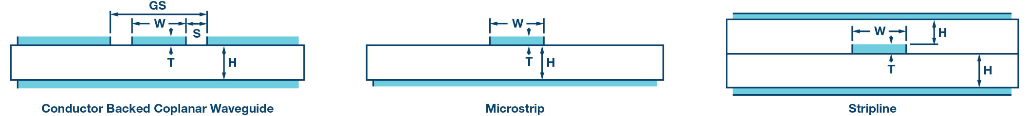
Different transmission line types produce different ?eff and vp. Using Equation 2, this means different transmission types of the same physical length have a different τpd. Table 1 and Figure 1 provide simulation results of three common transmission line types—CB-CPW, microstrip, and stripline that highlight the differences in ?eff, vp, and τpd. This simulation estimates τpd for a 10 cm CB-CPW trace is 100 ps greater than a stripline trace of the same length. Simulations were generated using the Microwave Impedance Calculator from Rogers Corporation.
Table 1. Rogers 4003C Simulation Results of Figure 1
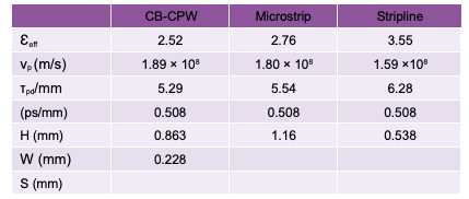
Rogers 4003C has a relative permeability (?r), also known as dielectric constant (Dk), of 3.55. In Table 1, note CB-CPW and microstrip have lower ?eff since they are exposed to air, whose ?r = 1.
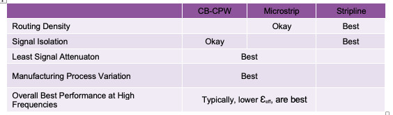
It is not always possible to route all delay matched signals on the same layer or with the same transmission line type. Table 2 provides some generalized considerations for selecting a transmission line type for different traces. If it is necessary to match τpd for different transmission line types, it is best to use a board simulation tool rather than hand calculations and rules of thumb.
Table 2. Generalized Transmission Line Considerations
Transmission Line VIAs
Recommendation: If a signal path has a via, remember to include the via length between the two signal layers of interest when calculating propagation delays.
For a rough propagation delay calculation, assume the via length connecting the two signal layers has the same phase velocity as the transmission line. For instance, a via connecting the top and bottom signal layers of a 62 mm thick board, would account for an additional τpd ~10 ps.
Adjacent Traces, Differential and Single-Ended Signals Recommendation: Keep a minimum of one line width between traces to avoid a significant change in ?eff.
Rules of Thumb:
- 100 Ω differential signals (odd mode) are faster than a 50 Ω single-ended signal.
- Closely spaced in-phase 50 Ω single-ended signals (even mode) are slower than a single 50 Ω single-ended signal.
The signal direction of closely spaced adjacent traces changes the ?eff and, as a result, the delay match between equal length traces. A simulation for two edge-coupled microstrip traces vs. a single microstrip trace are provided in Figure 2 and Table 3. This simulation estimates that the τpd for two 10 cm edge-coupled even mode traces is 16 ps greater than a standalone single trace of the same length.
When trying to match single-ended τpd to differential τpd, it is important to simulate the phase velocity of both paths. In clocking applications, this situation may occur when trying to send a CMOS sync or SYSREF request signal that is time aligned to a differential reference or clock signal. Increasing the spacing between the differential signal paths creates a closer phase velocity match between the differential and single-ended signals. However, this is at the expense of the differential signal’s common mode noise rejection, which keeps clock jitter to a minimum.
It is also important to point out that closely spaced in-phase signals (even mode) increase the ?eff, resulting in a longer τpd. This occurs when multiple copies of single-ended signals are route closely together.
Table 3. Adjacent Traces vs. Isolated Trace


Delay Match vs. Frequency
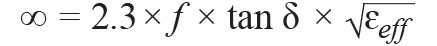
Recommendation: To minimize frequency related delay matching errors, choose a low Dk, low dissipation factor (DF) material (Dk <3.7, DF <0.005). DF is also known as loss tangent (tan δ) (see Equation 6). For multi-GHz traces, avoid plating technologies that include nickel.
Matching signal delays to the picosecond level of different frequency signals is challenging due to counteracting variables. Figure 3 shows that with increasing frequencies, dielectric constants typically decrease. Based on Equations 1 and 2 above, this behavior produces a smaller τpd as frequencies increase. Based on Equation 3 and the Roger’s material in Figure 3,1 the Δτpd between a 1 GHz and 20 GHz sine wave on a 10 cm trace is roughly 4 ps.
Figure 3 also shows signal attenuation increases as frequency increases, resulting in larger attenuation of a square wave’s higher order harmonic when compared to the fundamental tone. To what degree this filtering occurs will result in varying levels of rise (τR) and fall (τF) times. A change in τR or τF presents the waveform to the receiving device’s clock input as a change in total delay, which is composed of the trace’s τpd and the signal’s τR/2 or τF/2. In addition, different frequency square waves may also have a different group delay. For these reasons, square waves are more challenging than sine waves when estimating delay matching between different frequencies.
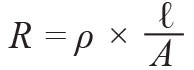
For more of a better understanding of attenuation (α in dB/ft) vs. frequency, refer to Equation 7 and Equation 8 and the references supplied in this article,2,3,4,5 which introduce loss tangents (δ) and skin effect. One key point from these references is that skin effect reduces the area (A) in Equation 8, which increases line resistances (R).3 To avoid excessive attenuation due to skin effect at high frequencies, avoid plating technologies that use nickel, such as solder mask over gold (SMOG) and electroless nickel immersion gold (ENIG) plating.4,5 One example of a plating technology that avoids nickel is solder mask over bare copper (SMOBC). To summarize, choose a low Dk/DF material, avoid plating technologies that use nickel, and run board-level delay simulations on key traces to improve delay matching of different frequencies.

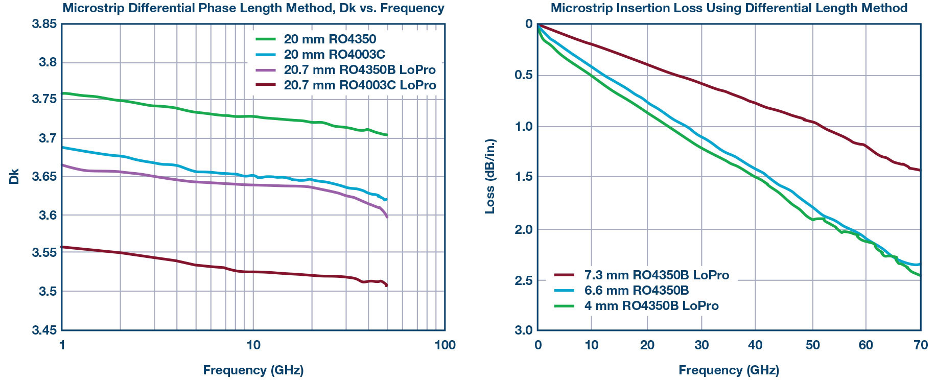 Dk and DF vs. frequency.1
Delay Match vs. Temperature
Recommendation: Choose a temperature stable dielectric material for PCB and cables. Temperature stable dielectrics typically have Δ?ppm <50 ppm.
Dielectric constants vary over temperature, which causes changes in a transmission line’s τpd. Equation 4 calculates Δτpd with respect to changes in the dielectric constant over temperature.
In general, PCB materials are lumped into two categories: woven glass (WG) or nonwoven glass. Woven glass materials are typically cheaper and exhibit a higher Dk, due to glass having a Dk = 6. Figure 4 compares Dk changes for a variety of different materials. Figure 4 highlights that some PTFE/WG-based materials have a steep TCDk between 10°C and 25°C.
Using Equation 3 and Figure 4, Table 4 calculates the Δτpd due to 25°C to 0°C temperature change of 10 cm stripline traces on different PCB materials. In a system that requires matching τpd across multiple traces at different temperatures, PCB material selection can cause τpd mismatches of a few picoseconds between 10 cm traces.
Coaxial cable dielectrics also have similar TCDk concerns. Coaxial cable lengths are usually much greater than PCB trace lengths, which will result in a much greater Δτpd over temperature. Using two 1 meter cables with the same properties shown in column 2 of Table 4 can create τpd mismatches of 25 ps when the temperature changes from 25°C to 0°C.
Table 4 assumes constant temperatures for the length of the 10 cm trace. In a real-world situation, the temperature may not be constant over the length of trace or coaxial cable, making analysis more complex than the scenario discussed above.
 Dk change vs. temperature.1
Table 4. Δτpd of 10 cm Stripline, 25°C to 0°C

Delay Matched Cables
Recommendation: Understand cost trade-offs between purchasing delay matched cables and the development cost of a calibration routine to adjust for delay mismatch electronically.
Based on the author’s experience, comparing coaxial cables of the same length and material from the same vendor results in delay mismatches in the 5 ps to 30 ps range. From discussions with cable vendors, this range is the result of variations that occur during cable cutting, SMA installation, and lot-to-lot variation of the Dk.
Many coaxial cable manufacturers offer phase matched cables within predetermined matched delay windows of 1 ps, 2 ps, or 3 ps. The price of the cable typically increases as the delay match accuracy increases. To manufacture <3 ps delay matched cables, manufacturers often add several delay measurement and cable cutting steps to their cable manufacturing process. For the cable manufacturer, these added steps result in increased manufacturing cost and yield loss.
Delay Match vs. Cable Bend
Recommendation: When selecting cable materials, understand trade-offs between delay shifts due to temperature vs. delay shift due to cable bends.
Bending coaxial cables results in different signal delays. Cable vendor data sheets often specify the phase error for 90° bend at a specific bend radius and frequency. For instance, an 8° phase change may be specified with a 90° bend at 18 GHz. Using Equation 5, this calculates roughly to 1.2 ps delay.
Delay Match vs. SMA Installation and Selection Variations in installation of PCB edge mount SMAs can add delay mismatch between clock paths, as shown in Figure 5. Errors of this nature are not measured typically and, as a result, are hard to quantify. However, it is reasonable to assume this could add 1 ps to 3 ps delay mismatch between clock paths.
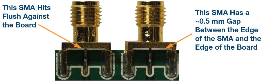 SMA installation delay mismatch.
One way to control delay mismatch due to SMA installation is to select SMAs with alignment features, as shown in Figure 6.
There is a trade-off since SMAs with alignment features are typically specified for higher frequencies than those without alignment features and, as a result, cost more. The SMA vendor often provides a recommended PCB to SMA launch board layout for the higher frequency SMAs. This recommended layout alone may be worth the additional price as it could save a board revision, especially if the clock frequency is >5 GHz.
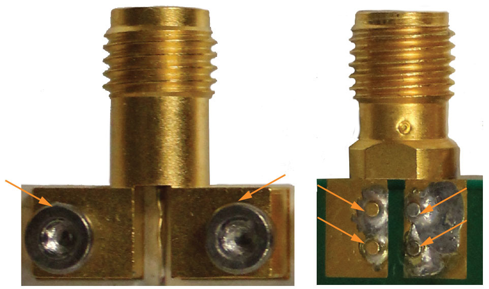 SMA with alignment features.
Delay Match Across Multiple PCBs
Recommendation: Understand the cost trade-off between purchasing PCB materials with well-controlled lot-to-lot ?r and the development cost of a calibration routine to adjust for delay mismatch electronically.
Trying to match τpd between traces on multiple PCBs adds several sources of error. Four of the sources of error were discussed above: delay match vs. temperature; delay matched cables; delay match vs. cable bend; and delay match vs. SMA installation and selection. The fifth source of error is process variation of ?r across multiple PCBs. Contact the PCB manufacturer to understand the process variation of ?r.
As an example, FR-4’s ?r can vary between 4.35 to 4.8.6 The extremes of this range produce a possible 35 ps Δτpd for 10 cm stripline traces on different PCBs. Other PCB material data sheets supply a smaller typical range for ?r. For instance, Rogers 4003C’s data sheet states an ?r range of 3.38 ± 0.05. The extremes of this range reduce the possible Δτpd to 9 ps for 10 cm stripline traces on different PCBs.
Clock Skew Due to Clock ICs
Recommendation: Consider newer PLL/VCO ICs that include <1 ps skew adjustments.
In the past, data converter clocks were generated from multiple output clock devices. The data sheets of these clock devices specified the device’s clock skew, typically ranging from 5 ps to 50 ps depending on the IC selected. To the author’s knowledge, none of the multioutput GHz clock ICs available at the time of this article provided the ability to adjust the clock delay on a per output basis.
As data converter clock frequencies >6 GHz become more common, single or dual output PLLs/VCOs will become the clock of choice. The advantage of the single output PLL/VCO clock IC architecture is that methods are being developed to adjust the reference input to clock output delays in <1 ps steps. The ability to adjust reference input to output delays on a per clock basis allows the end user to perform a system-level calibration to minimize clock skew to <1 ps. This sort of system level clock skew calibration has the potential to relax all PCB, cable, and connector delay matching concerns discussed in this article, and as a result will lower the overall BOM cost of system.
Conclusion
Several sources of possible delay variation and delay mismatch have been discussed. It has been shown that ?eff may vary with temperature, frequency, process, transmission line types, and line spacing. It has also been shown that a multi-PCB setup connected via coaxial cables creates additional sources of delay variation. When selecting material to minimize clock skew in a large clock tree, it is very important to understand how different PCB and cable ?r varies with temperature, process, and frequency. With all these variables, it would be difficult to design a large clock with <10 ps skew without some sort of skew calibration. In addition, purchasing PCB materials, coaxial cables, and SMA connectors to minimize clock skew would add significant material cost. To help ease calibration methods and lower system cost, many of the newer PLL/VCO and clock devices from IC manufacturers allow for sub-1 ps delay adjustment capability.
Table 5 provides a summary of the recommendations discussed in this document to minimize clock skew.
Table 5. Summary Recommendations to Minimize Clock Skew by Topic

References
1 Data supplied compliments of Rogers Corporation, used with permission.
2 Rick Hartley. “Base Materials for High Speed, High Frequency PC Boards.” PCB & A, March 2002.
3 Howard Johnson. “Skin Effect Calculation.” High Speed Digital Design, Signal Cosulting, Inc, 1997.
4 Howard Johnson. “Nickel-Plated Traces.” High Speed Digital Design Online Newsletter, Vol. 5, Issue 6, 2002.
5 Howard Johnson. “Nickel Matters.” EDN, 23 October, 2012.
6 “FR-4.” Microwaves101, 2018
Chris Pearson [[email protected]] graduated from Purdue University with a degree in electrical engineering. He is currently a senior applications engineer in Analog Devices’ Broad Market Frequency Generation Group, with a focus on high speed converter clocks. When not spending time at work or with his family, Chris enjoys practicing percussive fingerstyle guitar techniques, trying different grilling recipes, and a variety of other outdoor activities.