
Understanding IoT requirements 101, part 1
April 04, 2017
Blog
To play in the Internet of Things (IoT) market, original equipment manufacturers (OEMs) need to be able to embrace a faster rate of innovation. The possible spectrum of IoT applications is...
To play in the Internet of Things (IoT) market, original equipment manufacturers (OEMs) need to be able to embrace a faster rate of innovation. The possible spectrum of IoT applications is endless, and successful companies enable their developers to continuously identify and implement new and more useful ways to harness the capabilities of sensors, monitor different types of data, and control ecosystems of devices.
IoT applications cross many domains, including wearables, cars, homes, industries, and even cities. In addition to allowing developers to implement innovation, IoT devices must be highly efficient, secure, and aesthetically pleasing. Applications are important and must be wrapped around intuitive software designed to promote easy-of-use devices.
Microcontrollers (MCUs) are at the core of IoT-based products, and selecting the right MCU is key to meeting the present and future needs of your customers. This article will explore the wide range of capabilities today’s embedded MCUs can provide to accelerate design while enabling innovative applications. In part 1, we will cover advanced process technology, low power design techniques, power considerations for multicore systems, inter-core communications, serial memory interfaces, and system security.
IoT market (the fastest growth engine)
IoT technology continues to transform everyday work and lifestyles to be more affordable, accessible, comfortable, and intelligent. The IoT market can be broadly classified under two categories: consumer IoT and business IoT.
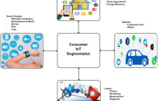
Consumer IoT
Consumer IoT broadly includes home, lifestyle, health, and mobility. Devices are often connected products for individuals to enhance their productivity, safety and lifestyle. From smart homes to connected cars, and from smart healthcare to comfort lifestyle, the consumer market is gearing up for the next big wave.
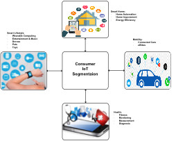
[Figure 1 | Consumer IoT market segmentation]
Business IoT
Business IoT is vast and broadly includes retail, health, energy, mobility, cities, manufacturing, and public services. The business IoT segment will transform organizations and communities to enable a new era of economic growth. The IoT does this by connecting data, people, and machines to improve productivity, efficiency, and day-to-day operations. Business IoT can also serve as a tool to help companies identify new growth opportunities in unexplored areas.
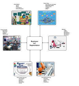
[Figure 2 | Business IoT market segmentation]
Process technology (size – a big deal)
The process technology used to manufacture an MCU is critical to determining its performance, low power capabilities, and cost. IoT applications require both efficient active power consumption and low-power mode consumption for overall power efficiency of the system. Continuing advancements in manufacturing technology have led to shrinking the die size. This reduces the overall cost of the chip, as it allows more MCUs to be manufactured on the same piece of silicon wafer. Performance and power are also directed impacted by die shrinking. Shrinking a die reduces the current required to switch each transistor on/off while maintaining the same clock frequency. As a result, smaller chips have lower power consumption with higher maximum clock frequency leading to higher performance.
For example, 40 nm process technology, such as is used to manufacture Cypress Semiconductors’ Programmable System-on-Chip (PSoC) 6 BLE-series MCUs, provides high performance and cost-efficient implementations for various IoT applications. Deep sleep current requires only few microampere with full retention. Other power modes, including active, sleep, low power active, and low power sleep, give developers the flexibility to optimize system power consumption while maintaining high performance when it is needed.
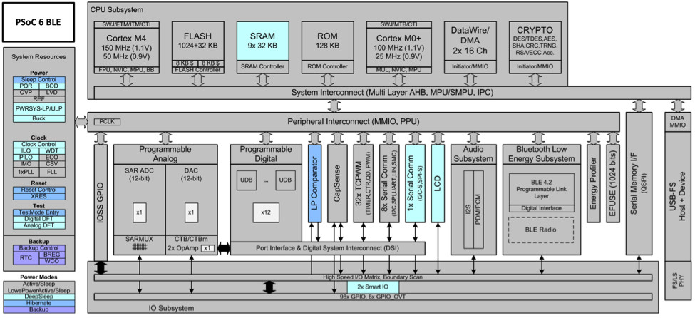
[Figure 3 | Block diagram of a low power MCU for an IoT application]
Power (it matters the most)
One of the great challenges when designing IoT devices is that they can be power-hungry. Most IoT devices are Always-On and Tiny, meaning they are limited in the size of battery they can hold. There are various factors that MCU vendors consider when optimizing an MCU for IoT applications, such as
- Improving the process technology
- Providing highly flexible power modes
- Enabling power-optimized hardware IP blocks
- Integrating important features into a single chip
- Optimizing the Flash access frequency
- Enabling cache memory
- Supporting a wider operating voltage range
Unfortunately, while shrinking the process technology improves performance, power, and integration, it introduces the challenge of managing leakage currents, especially in low power modes. To address the challenge of leakage currents, MCU vendors employ special transistor process techniques such as multi-gate devices, high voltage transistors/logics/circuits, specially designed memory cells, and others.
The availability of flexible power modes enables developers to schedule individual system events such that the overall power consumption is optimized. A key technique is to provide multiple peripherals which can operate in low power modes and that can be woken up to perform their function without having to wake the CPU. Some MCUs also provide a special low power active mode wherein peripherals are available for operation with limited features (such as lower operating frequency and voltage) to further optimize application power consumption. Even specific peripherals can be designed for optimized power consumption; i.e., a BLE radio can be designed to support low power wireless communication.
Another element that impacts power consumption significantly is non-volatile (NV) memory access. This is true in particular to MCU where Flash (NV memory) is used to store firmware code. Any optimization in Flash access results in substantial power reduction. The objective is to minimize the frequency of Flash access. There are two common techniques applied here. One method is to provide a cache memory. In this way, the actual code memory (Flash) does not need not to be accessed for every cycle of execution. Another method is to increase the amount of data fetched in one-cycle. Using wider Flash access reduces Flash access frequency.
IoT-based MCUs may also provide a flexible power system. By supporting a wide supply voltage range, the MCU can be powered using multiple sources. For example, a simple IoT application such as a fitness tracker can be powered by a coin cell, while complex IoT applications such as smartwatch can be powered by power management integrated circuits PMICs. Some MCUs offer an internal buck converter to regulate the power efficiently.
When considering the power modes of an MCU, it is important to look beyond the base architecture. For example, the standard ARM CPU core supports active, sleep, and deep sleep. Additional power modes are often added by the specific MCU supplier. For example, the Cypress PSoC 6 BLE MCU operates in six power modes, adding low power active, low power sleep, and hibernate.

[Figure 4 | Power mode transitions example in PSoC 6 BLE MCU]
Multiprocessor MCUs (running parallel applications task faster)
IoT systems are simultaneously growing in complexity based on their feature set while at the same time shrinking in terms of physical size. MCU manufacturers aim to improve the performance of the system while keeping size and power as low as possible. Multicore MCUs and system on chips (SoCs) provide higher performance by integrating more functions in a single chip and minimizing chip real-estate. A multicore processor is an MCU or SoC comprising two or more independent cores (or CPUs). The cores are typically integrated onto a single chip, although they may be implemented as multiple dies in a single package.
Multicore MCUs can help provide high performance while maintaining a small footprint. In a typical IoT design such as wearable device, more than one MCU is required: a BLE controller for wireless communication, Touch MCU for the user interface implementation, and a primary MCU to run the application. The functionality of these three MCUs can be provided through a single highly-integrated multicore MCU.
Multicore MCUs provide many other benefits. For example, multicore MCUs integrate enough resources to allow the CPUs to handle intensive tasks in parallel and so take advantage of multitasking efficiencies. These also allow developers to efficiently assign system events to a specific core such that the power and performance goals are met. For example, in a dual-core wearable design, periodic functions such as wireless broadcasting and touch sensing that need less CPU intervention can be assigned to one core. Other “high-touch” functions such as sensor fusion which require extensive CPU intervention can be assigned to another core. Such partitioning reduces lag time when running more than one application in a system. Integration also improves efficiency by consolidating protocol stacks and program memory.
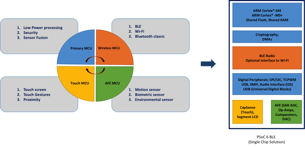
[Figure 5 | An example of a multicore MCU for IoT applications]
Figure 6 shows a multicore MCU, the Cypress MCU PSoC 6 BLE. This dual-core device has two 32-bit ARM Cortex CPUs, the Cortex- M4 and Cortex-M0+. Both these CPUs are 32-bit processors with a 32-bit data path, 32-bit registers, and a 32-bit memory interface. The Cortex-M4 is the main CPU designed for short interrupt response time, high code density, and high 32-bit throughput while maintaining a strict cost and power consumption budget. The Cortex-M0+ serves as a secondary CPU that handles security, safety, and protection features. Cortex CPUs implement a subset of the Thumb instruction set and have two operating modes called Thread Mode and Handler Mode. These CPUs enter Thread Mode when they come out of reset and execute application software. To handle exceptions, the CPU enters Handle operating mode. After all exception processing is complete, the CPUs returns to Thread mode.

[Figure 6 | Multicore embedded MCU example (PSoC 6 BLE)]
Inter processor communication (enables peripheral sharing and exchange of information)
In multi-core MCUs, inter processor communication (IPC) is required to coordinate operations between the cores. IPC serves as a communication manager handling the distribution of messages between processors. Modern CPU architectures such as the ARM Cortex support multicore communication in hardware and firmware. One such example is an send event (SEV) instruction which asserts all the cores in a device when executed. Various methods have been adopted by MCU vendors to implement IPC:
Interrupt based
With this approach, one core sends an interrupt to the other core to indicate an application event. Typically, the interrupt routine is very compact and doesn’t occupy much code memory. As with any interrupt mechanism, each interrupt has its own interrupt service routine (ISR) through which specific tasks can be executed by the respective core. For the actual passing of data, there is a shared memory that can be accessed by multiple cores. In addition to sharing data, it provides a mechanism for requesting and acknowledging messages.
Mailbox
A Mailbox is a dedicated memory space in RAM for each CPU to send and receive messages with one another. Each core maintains its own RAM memory (mailbox) and send messages to other cores’ mailboxes.
Message queue
A message queue uses two areas of shared memory to store the messages that each core sends to the other. The first is a dedicated memory called the command buffer that stores commands sent from the master to the slave. The other dedicated memory is called the Message Buffer and allows the slave to respond to the master.

[Figure 7 | Various modes of Inter Processor Communication (IPC)]
Semaphores
Semaphores are a mechanism to prevent multiple sources from accessing a shared resource at the same time. In a multicore processor, shared hardware locations act as a semaphores to indicate, for example, whether a particular shared peripheral is being used by a specific core. Before accessing the peripheral, other cores in the system read the semaphore status to see if it is available.
Serial memory interface (IoT memory of choice)
Memory is an integral part of any IoT system and is used for both code and data storage. The ever-growing intelligence required in modern IoT devices drives the need for larger code and data memory. However, integrating all of this memory as internal memory to the device would increase the die-size and cost of the MCU. An alternate approach is to provide the option to expand the memory externally as needed. This enables developers to add memory according to the needs of the end application. In addition, if during the course of development cycle it turns out the budgeted internal memory space is not sufficient, additional external memory can be introduced without having to redesign the entire system.
It is also important to be aware of the speed and security of the external memory interface, as well as how easy it is to use. In general, serial memory is the better choice over parallel memories to conserve limited IO pins on the MCU. While SPI-based serial memories offer reasonable interface speed for data logging, higher speeds are needed for direct external code execution. These requirements have pushed MCU manufacturers to provide alternatives to SPI. Here is a quick comparison of data throughput of different schemes.
- SPI: Supports 1 bit/cycle throughput
- Dual-SPI: Supports 2 bits/cycle throughput
- Quad-SPI: Supports 4 bits/cycle throughput
- Dual Quad-SPI: Supports 1 byte/cycle throughput
Typically, an MCU will support multiple types of memories simultaneously to give developers the most flexibility.
Since many IoT systems handle a user’s personal data, it is important to ensure data security. Similarly, code memory needs protection to prevent unauthorized use of the device. External memories are more vulnerable on this aspect of security, so special mechanisms are required to protect externally stored data. To achieve this, MCUs use various encryption techniques (e.g. AES, DES, RSA) to protect data and code from unauthorized access. For example, the PSoC 6 BLE MCU from Cypress semiconductor offers a special serial memory interface (SMIF) peripheral that supports both execute in place (XIP) mode for direct external code execution and memo mapped IO (MMIO) mode for data logging. It is controlled using special commands such as program/erase of Flash, sleep mode entry for memory devices, etc.

[Figure 8 | Example of a serial memory interface (SMIF)]
The SMIF allows users to configure multiple memory devices of the same or different type and size. Multiple memory devices are be mapped to different addresses in the memory (XIP) mode. They can be different memory types, aligning them to different purposes in the system. They can also be identical memory devices configured in consecutive address spaces to simulate a continuous large memory. Using the SMIF peripheral in combination with SPI Flash memory is a viable replacement for external NAND and NOR flash memory and can save board space as well. Ease-of-use is improved over NAND memory as serial Flash maps directly into the processor’s memory space data storage as well as supports execute XIP.
System security, privacy, and safety (root of trust)
Once a device is connected, the possibility of being hacked is introduced. Thus, the security of IoT devices is a non-negotiable element, whether the device is a personal wearable band or a connected car. Data protection is needed at all levels, including storage, processing, and during communications to ensure system reliability. In addition, any software or firmware that handles data should also be secured. Such security can be enabled on two levels. The first level is security by software. The second level is security by hardware, i.e. protect the software through hardware.
Typically, software-based security uses secret keys stored within the code space. Though this technically works to perform encryption and decryption, the process is still vulnerable to hacking as it is a stored code. The moment the code is decoded, security is defeated.
Hardware-based security uses integrated circuitry to protect the system; for example, the encryption and decryption of code and data. Hardware-based security is self-contained and does not need any additional software to operate, eliminating the possibility of malicious code, infection, contamination, or other vulnerabilities from compromising the system, customer data, and services. For this reason, hardware-based security is the preferred approach when protecting sensitive data or code. This is why MCUs for IoT applications have sophisticated integrated hardware security features such as cryptography blocks, code protection IP, and other hardware-based mechanisms.
Hardware-based security also has the added benefit of providing faster performance with lower power compared to firmware implementations. For example, the dedicated cryptographic block in the Cypress PSoC 6 BLE MCU accelerates cryptographic functions. In addition, the block provides True Random Number generation functionality, symmetric key encryption and decryption, hashing, message authentication, random number generation (pseudo and true), cyclic redundancy checking, and utility functions such as enable/disable, interrupt settings, and flags. This MCU device is also equipped with secure boot functionality. Secure boot uses ROM routines to guarantee the authentication of user data in Flash. A secure boot is a process involving cryptography that allows an IoT device to start executing authenticated and therefore trusted software to operate. Thus the system can power on from a known, trusted state.
In part 1, we have covered advanced process technology, low power design techniques, power considerations for multicore systems, inter-core communications, serial memory interfaces, and system security. In part 2, we will cover advanced BLE wireless links, analog front end, smart touch interface, and other technologies important to IoT design.

[Figure 9 | Security ecosystem in MCU for IoT applications]


