Embedding flexible analog interface IP into digital SoCs
November 01, 2010

Internal data converters in an analog interface must maintain flexible connectivity and compatibility with multiple wireless standards.
More and more analog and mixed-signal capability is being integrated into Systems-on-Chip, including baseband RF functions. Careful attention to detail is needed to maintain circuit performance and deliver functionality while keeping power consumption low. Designers can explore the criteria for a flexible analog interface to build a successful wireless communications device.
Today’s consumers are getting more and more sophisticated. They are now creators of their own content, like HDTV videos or large sets of digital photographs. They expect to be able to share it anytime, anywhere, with anybody, and without delay; they do not want to be limited by slow wired connections.
These consumers are driving the implementation of broadband wireless network terminals in every conceivable device, beyond the traditional mobile phone and into the PC, TV, car, camcorder, and even picture frames.
To serve this consumer expectation, terminal devices must be cost-effective and simple to use. In addition, the wireless transceiver in these devices should be compatible with all broadband communication standards, including Long-Term Evolution (LTE), WiMAX, and Wi-Fi. These goals can be achieved by carefully defining the analog interface’s characteristics and internal components, paying attention to several details.
The wireless baseband analog interface
A traditional communications system (Figure 1) comprises an analog RF block to translate over-the-air communication into baseband (BB) analog signals and a digital BB processor block to translate modulated signals into meaningful communication content. A wireless BB analog interface translates signals between the analog and digital domains.
|
|

To implement interchip communication between the digital System-on-Chip (SoC) with an external RF chip (RFIC), the analog interface is typically integrated with the digital BB processor in a complex digital SoC.
The analog interface comprises an IQ-Analog-to-Digital Converter (ADC) in the receive path and an IQ-Digital-to-Analog Converter (DAC) in the transmit path. It also includes an auxiliary ADC and an auxiliary DAC for measurement and control purposes. A Phase-Lock-Loop (PLL), which generates the sampling clock for all these converters, can also be considered part of the interface.
Most modern implementations of wireless communications transceivers are multi-antenna array (Multiple In, Multiple Out or MIMO). In these cases, the receive and transmit paths use multiple instantiations of an IQ-ADC and IQ-DAC (one per antenna). These architectures implement advanced processing techniques such as diversity or special multiplexing to improve communication quality.
Embedding a flexible analog interface into a digital SoC
To implement multiple communication standards and enable the BB chip to be used with any RFIC, the analog interface must be very flexible. The definition of the interface and the internal data converters should take this into account to facilitate the analog interface’s integration inside the digital SoC. The following ground rules should be followed:
- The interface should be compatible with multiple wireless communication standards while keeping power dissipation at a minimum.
- The interface should be flexible, allowing seamless connection between the BB chip and any external RFIC without requiring additional external circuitry.
The system designer should thus look beyond the basic characteristics of a data converter IP (area, power dissipation, throughput, dynamic range) and into the detailed characteristics that make it flexible and easy to integrate.
Compatibility with multiple standards
It is interesting to observe that most broadband wireless communication standards have defined a similar set of performance characteristics for the analog interface. In fact, most protocols define a maximum communication channel width at 20 MHz (or 40 MHz for Wi-Fi 802.11n). Furthermore, the conversion resolution required is typically 10- or 12-bit. This means a data converter with these characteristics is effectively compatible with multiple protocols. However, the optimal sampling rate for different communication modes within the same protocol (LTE mode 1 or mode 6, for example) may differ.
The communications system should be configured such that the same hardware can be used in all modes in the most power-efficient way. For the data converters in the analog interface, this means they should allow operation at a wide range of sampling rates without performance variation. Furthermore, operation at low sampling rates should not penalize the system’s energy efficiency; the converter’s power dissipation should be proportional to the sampling rate while maintaining performance, as shown in Figure 2.
|
|

Optimal interface with the RFIC (ADC/DAC)
For the highest system flexibility, the BB processor chip should be implemented in a way that does not impose restrictions on the RFIC connected to it.
Systems are typically implemented using a DC-coupled zero IF demodulation scheme. The analog signal level coming out of the RF block is not known and varies for different vendors.
To communicate seamlessly with all RFICs, the data converters in the analog interface need to support a wide range of input signal common mode voltages and perform the signal-level translation in its internal signaling levels without the need for extra external components (coupling capacitors or operational amplifiers).
For the receive path, dedicated level-shifting circuitry in the ADC sample and hold can implement all these functions and thus guarantee maximum interface flexibility. Figure 3 shows an example of an ADC input stage that can process signals with a wide range of common mode levels.
|
|

In the transmit path, a DAC using a current steering architecture enables the level translation function to be implemented without further overhead.
It is possible to alleviate the complexity of the analog reconstruction filter and thus simplify the RF block by using the transmit DAC at a higher sampling rate to increase signal oversampling. However, this solution is only viable if the DAC’s power dissipation and performance are not affected by the higher sampling rate.
Support for 2G/3G/4G communications
A special category of wireless communication modems must support communications based on protocols for multiple generations (2G, 3G, and 4G), such as in the context of cellular applications. Modems for cellular applications must implement widely different requirements using the same hardware, for example:
- Narrowband Gaussian-filtered Minimum Shift Keying (GMSK) with 200 kHz channel bandwidth requires ADC performance in excess of 74 dB Signal to Noise and Distortion Ratio (SNDR).
- Broadband LTE with up to 20 MHz channel bandwidth requires ADC performance in excess of 63 dB SNDR.
The optimal solution for these modems is to implement the ADC using a wideband sigma-delta architecture. These converters are designed using a highly programmable analog sigma-delta modulator, followed by programmable digital filters. This embedded programmability allows trading off speed (signal bandwidth) and dynamic range (SNDR) while maintaining the power dissipation at a minimum. Additionally, due to the high oversampling rate, the analog anti-aliasing filters present in the RF block can be simplified.
Processing large bandwidth analog signals
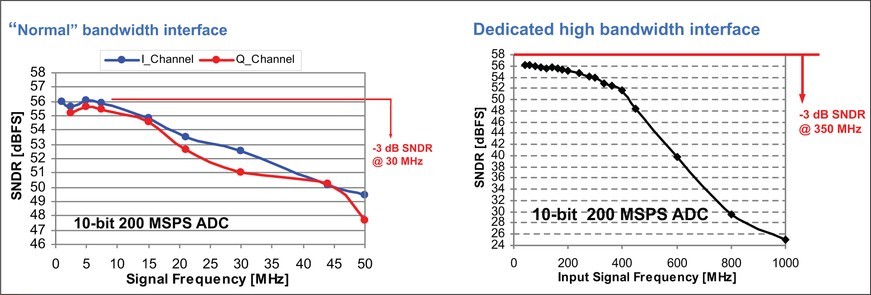
The most common demodulation technique used for broadband wireless communications is based on a zero/near-zero IF implementation. However, in some cases, IF demodulation is preferred. In these situations, the IF signal is digitized and processed directly in the digital domain, thus simplifying the analog RF circuitry. In IF demodulation, the communication channel band to be digitized by the ADC is centered on a high frequency (the IF frequency).
To digitize these signals, the ADC input must be able to sample high-frequency signals while not jeopardizing the ADC’s performance. Traditional converters for baseband applications exhibit performance degradation for high-frequency input signals. An ADC that integrates a dedicated high-frequency input stage targeting high-frequency signals can overcome this limitation (see Figure 4).
|
|
Ready-to-integrate IP
Achieving a successful design that integrates broadband wireless communications interfaces in a digital SoC depends on the definition of the analog interface and a careful selection of the blocks that make up the interface. Selection should look beyond the common criteria of resolution/performance and take into account the features embedded in these converters that help build a flexible solution. These converters should seamlessly communicate with any RFIC and accommodate all common broadband communication standards in the most power-effective way using the same hardware.
Synopsys DesignWare Data Converters were created in view of such needs. Synposys offers a complete portfolio of analog interface solutions that greatly simplifies its integration in a digital BB processor SoC.
Synopsys 650-584-5000 [email protected] www.synopsys.com