
Formal Verification Flow, Benefits, and Debug on 16 nm Technology
September 15, 2020
Story

Initial netlists in a formal verification process must be optimized, so additional logic is needed for Design for Test. Here we offer formal verification flow and debugging techniques for 16 nm node.
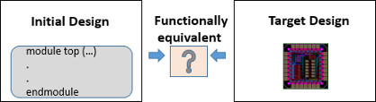
Formal verification is the process of comparing two designs written in a hardware description language (HDL) to ensure they are functionally equivalent. A subset of functional verification, it provides a critical first step in checking the functional equivalence of two designs without using simulation.
The first of these functional equivalents is called a reference design/golden design, from which a model based on register transfer-level (RTL) code such as Verilog, System Verilog, or VHDL is used as a reference netlist. This netlist is verified against a corresponding netlist in the second design, known as the implementation or revised design (Figure 1). For the sake of simplicity, the reference/golden design will be referred to as the "Initial Design" for the remainder of this article, and the implementation design/revised design referred to as the "Target Design."
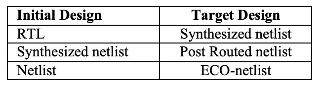
The following table shows a combination that can be used for comparison of the Initial Design with the Target Design.
This process requires that the initial netlist go through various levels of optimization, which in turn requires additional design for test (DFT) logic. Despite these requirements, the formal verification process should not alter the logic functionality of the design.
Types of Formal Verification
Two formal verification techniques are generally used:
- Equivalence checking – Logic equivalence checking is a technique that takes two designs that can have either the same or different levels of abstraction (i.e., algorithmic, RTL, or gate level) and checks for any functional differences between them.
Equivalence checking is further classified as either combinational or sequential. Combinational equivalence checking consists of checking the combinational logic by mapping one-to-one flops from the Initial Design to the Target Design, whereas sequential equivalence checking is used if there is different combinational logic between one-to-one flop mapping but the design should still be able to produce same output if given the same input. Generally, sequential equivalence checks are used if the SoC or ASIC design has undergone various transformations like retiming, power-saving design optimizations, etc.
- Property checking or assertion-based verification (ABV) – Property checking or ABV checks that a behavior is or is not possible, and uses a property checker tool to prove that the design meets all of its specifications. Property checking uses mathematical procedures to prove the accuracy of the design.
Two property languages are generally used for property checking: interval temporal logic (ITL) and System Verilog Assertion (SVA). Once these are coded, they can be passed on to the mathematical tool, which predicts the outcome as holding or failing. A holding ITL/SVA means all of the properties have been checked and holds the properties of the initial design. Failing ITL/SVA means the design behavior was not intended and that the target design has violations.
Requirements of Formal Verification
A functional equivalence check usually requires simulation of the two HDL designs using the same test vector. But, as ASIC technology shrinks and the complexity of circuits increases, it's not possible to use simulation to verify circuit functionality because the simulations might run for months. Therefore, formal verification plays a very important role by saving simulation run time as the well the huge resource requirements of those extended simulations.
Also, as the design goes through various stages from synthesis, place and route, sign-offs, and engineering change orders (ECOs), the formal verification must ensure that circuit logic functionality will not be impacted by any of the stages.
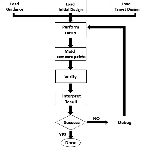
The flow for formal verification is pictured below.
Steps of Formal Verification
The following steps are performed during formal verification:
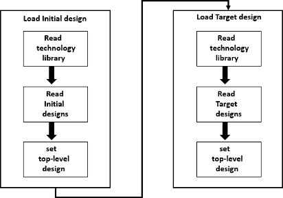
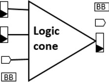
Read – The read step reads both the Initial design and Target design, as well as all the related technology libraries (Figure 3). It further partitions the design into the key equivalence checking concepts of logic cones and compare points:
- Common compare points: Input of a black box; Register or latch; Primary output
- Less common compare points: Multi-driven net; Loop; Cut-point
- Logic cones (Figure 4): A block of combinational logic that drives a compare point
Setup – The synthesis tool provides all of the automated setup information, including clock gating and scan insertion, which is recognized by the formal verification.
Match – The matching process will first try to verify the guidance file and apply any guidance that has been set. The match will also try to match compare points based on the following:
- Name-based algorithms
- Signature-based analysis
- Note: Any unmatched points are then reported.
?Verify – The verification cycle verifies logic equivalence for each logic cone of the reference design with the corresponding Implementation design. Formal verification algorithms use many solvers to prove equivalence or non-equivalence. There are four possible results:
- Succeeded: The implementation is equivalent to the reference
- Failed: The implementation is not equal to reference, meaning there are logic difference or setup problems.
- Inconclusive: No points failed but analysis the analysis did not completed, which might be due to time out or complexity.
- Not Run: Due to some initial problem in the flow, verification failed to run.
Debug-
- Checks for any warning signs.
- Checks for any rejected SVF guidance commands.
- Checks for unmatched compare points.
Analysis of Report and Fixes
Once a formal verification run is complete, a report analysis can be generated and fixes can be performed, if necessary.
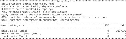
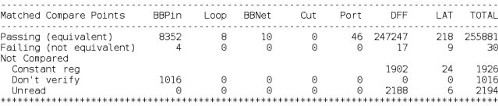
Figure 5 below shows the matching report. Here, a total of 30 failing compare points have been reported, including four Black Box Pins (BBPins), 17 D Flip Flops (DFFs), and nine latches. In addition, the report indicates a verification failure (Figure 6).
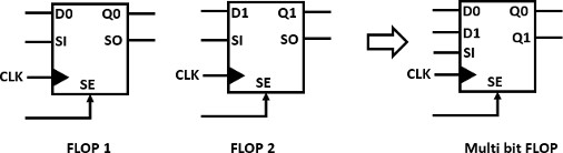
Because there might be some conversion happening from a normal flop to a multi-bit flop, resulting in the flop being reported as a non-equivalent point, DFF represents a potential fix.
Benefits
- No need to run simulation.
- Functionality checks can be done by taking a netlist after any stage.
- Bugs can be easily identified.
Conclusion
This paper gives an introduction to formal verification flow, techniques used in formal verification, and debugging 16 nm technology nodes. Formal verification can easily detect any bugs or logic failures that might have occurred during timing fixes, ECO implementations, or any back-end process.
References
- https://solvnet.synopsys.com/dow retrieve/O- 2018.09/dg/forolh/Default.htm
- https://support.cadence.com/
About Authors:
Nitin works for eInfochips (an Arrow Company) Physical Design team, and has worked on PnR and Physical verification.
Dr. Rajendra Pratap works in eInfochips' (an Arrow Company) Physical Design team, bringing more than 22 years of experience. He has experience taping out multiple physical designs.


