
How to develop tiny solar-powered wireless sensor nodes
September 07, 2017

The best practice for designing battery-free devices is to reduce the average power consumption of the wireless sensor system. This can be done through technologies such as Bluetooth Low Energy.
Wireless sensor nodes promise to reduce implementation costs by reducing the size of sensors, simplifying maintenance issues, and maximizing battery life. However, even greater growth will be possible with an emphasis on battery-free implementations.
The best practice for designing battery-free devices is to reduce the average power consumption of the wireless sensor system. This can be done through technologies such as Bluetooth Low Energy (BLE) for communications and energy harvesting.
Figure 1 shows the architecture of a tiny wireless sensor. This sensor is built around a microcontroller (MCU) with integrated BLE radio that can operate entirely using power from an energy harvesting power management integrated circuit (IC).
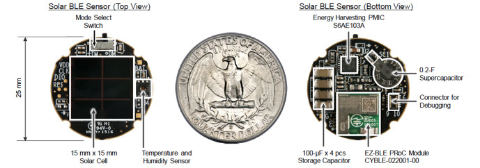
[Figure 1 | A tiny wireless sensor is built around an MCU with integrated BLE radio optimized to operate using only power from an energy harvesting power management IC. Shown here is the CYALKIT-E02 Solar-Powered BLE Sensor Beacon RDK which shows a complete wireless sensor.]
Optimizing Bluetooth Low Energy
To be able to operate using only power from energy harvesting, a sensor must optimize its BLE implementation to minimize power consumption. To achieve this, designers must first understand the implementation details of the BLE subsystem. Next, firmware needs to be written to match the requirements of each operating/power mode. Then, designers must analyze actual power consumption to confirm assumptions and further improve power efficiency of the system.
These techniques for reducing power consumption will be illustrated using the CYALKIT-E02 Solar-Powered BLE Sensor Beacon Reference Design Kit (RDK) from Cypress. This RDK includes the Cypress PSoC 4 BLE and S6AE10xA Energy Harvesting Power Management IC (PMIC).
First, let us consider a simple BLE design without power optimization. The BLE radio is configured as a beacon in non-connectable advertisement mode. A BLE beacon is a one-way communication method that broadcasts at a regular interval. It consists of small packets of data (30 bytes) that are sent as part of the advertisement packet. Beacons that want to be discovered can be used for a variety of smartphone or computer applications to trigger actions such as push messages, app actions, and prompts.
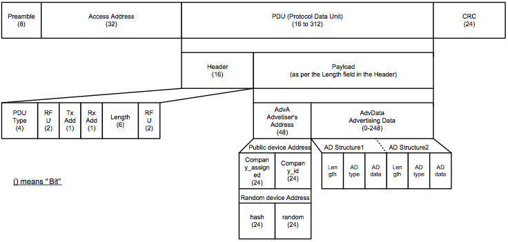
Figure 2 shows a link layer format of Bluetooth Low Energy for Advertising channel packet format. The link layer of Bluetooth Low Energy has “Preamble”, “Access Address”, “Protocol Data Unit (PDU)” and “Cyclic Redundancy Code (CRC)”. Note that the following information is for the advertising channel packet format and does not include “Data Channel Packets.”
- "Preamble" must set "10101010b"
- "Access Address" must be set to "10001110100010011011111011010110b (0x8E89BED6)"
- "PDU" has "Header" and "Payload"
The packet structure of a BLE beacon belongs to "Advertising Data" in "Payload".
[Figure 2 | Link layer format of BLE for advertising channel packet format.]

[Figure 3 | BLE beacon packet format]

Table 1 shows the setting values.
To determine how efficient the BLE design is, we can calculate the average consumption current using the voltage and current waveform. Figure 4 shows the energy results of the non-power optimized design.
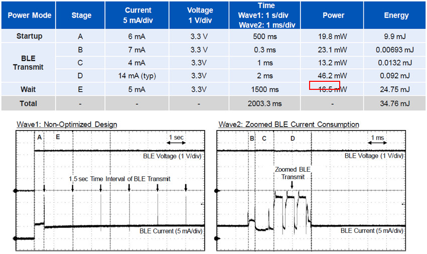
[Figure 4 | Current consumption of BLE design without power optimization]
The average current is about 5 mA, and total consumed energy from startup to wait is 34.76 mJ. To operate using environment energy, we will need to reduce the consumption current.
Optimizing firmware for low power
We can reduce the average current consumption of the BLE design by optimizing the following four functions:
- Low-power startup
- Deep-sleep
- IMO clock setting
- Debug select
To do so, we need to utilize a watch dog timer (WDT) to wake up the system when the system is in low power mode.
Low-power startup
After a power-on-reset (POR), the BLE system initializes various components by calling their respective start functions. Perform the following steps at initialization for low-power operation:
- Shut down the 24-MHz external crystal oscillator (ECO) to reduce power consumption while the 32.768-kHz watch crystal oscillator (WCO) is starting.
- Enable the WDT to wake up the system after 500 ms (WCO startup time).
- Configure the MCU in deep-sleep mode for the 500 ms WCO startup time.
- After the WCO is enabled, restart the ECO to enable the BLE subsystem (BLESS) interface.
- Set the WCO to low-power mode and change the low frequency clock (LFCLK) source from the 32‐kHz internal low-speed oscillator (ILO) to the WCO.
- Enable the WDT to wake up the system.
- Configure the MCU in deep-sleep mode.

[Figure 5 | Low-power startup waveform]
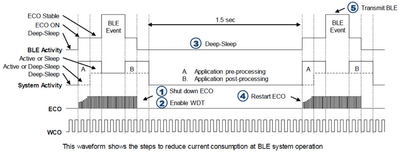
Deep-sleep
The user design should manage the system clocks, system power modes, and BLESS power modes to implement low-power operation in BLE-enabled MCUs.
The following steps are recommended to implement deep-sleep between BLE intervals:
- Shut down the ECO to reduce power consumption.
- Enable the WDT to wake up the system after 1.5 sec (BLE event interval).
- Configure the MCU in deep-sleep mode.
- After 1.5 sec, restart the ECO to enable the BLESS interface.
- Transmit the BLE advertisement data.
- Repeat from step 1.
[Figure 6 | Deep-sleep waveform]
IMO clock setting
The 3-MHz to 48-MHz internal main oscillator (IMO) is the primary source of internal clocking. The IMO default frequency is 48 MHz and it can be adjusted between 3 MHz to 48 MHz in steps of 1 MHz. The IMO tolerance with the RDK in this example with the default calibration settings is ±2%. 7 shows an example of total energy by changing IMO frequency.
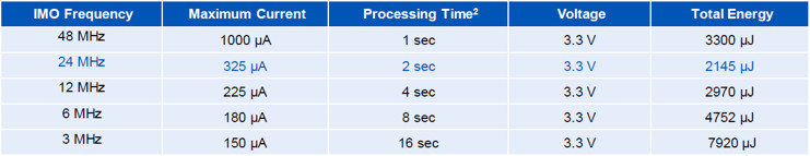
[Figure 7 | IMO DC specifications and example total energy]
Debug select
The serial wire debug (SWD) pins are used for run-time firmware debug during development stages. Configuring the SWD pins for debugging increases the current consumption. Therefore, in the production release, they should be switched to general purpose input/output (GPIO) mode. This makes them still available for device programming on chip reset.
To confirm how much we have optimized the design, calculate the average consumption current of the optimized BLE design using the voltage and current waveform. Figure 8 shows the energy results of the power optimized design.
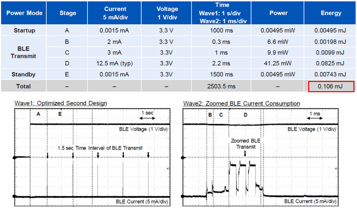
[Figure 8 | Current consumption of BLE design with power optimization]
The average current is about 1.5 µA, and total consumed energy from startup to wait is 0.106 mJ.
Operating using energy harvesting
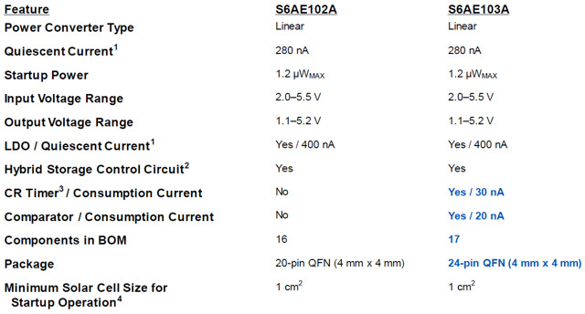
Now we need to confirm that the system can operate on energy harvesting technology at this level of average current and total energy consumption. Figure 9 shows a block diagram of the energy harvesting system. This system utilizes the S6AE10xA Energy Harvesting (EH) PMIC family and can operate for an entire day using the CYALKIT-E04 S6AE102A and S6AE103A EVK in conjunction with the CY8CKIT-042-BLE BLE Pioneer Kit.
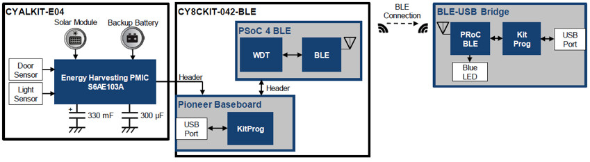
[Figure 9 | Energy harvesting system block diagram]
The block diagram in Figure 10 shows simple energy harvesting operation with a PSoC 4 BLE, which is supported by the S6AE102A and S6AE103A boards.
Wave1 highlights BLE operation using solar energy and Wave2 shows BLE current consumption while transmitting. The PMIC first stores solar energy in a storage device on VSTORE1 (VST1), which is a 300-μF ceramic capacitor. When VST1 achieves VVOUTH, the energy is sent to the MCU for BLE operation.
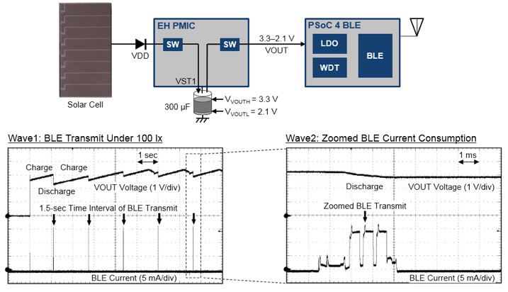
[Figure 10 | Simple energy harvesting]
However, such simple energy harvesting cannot operate for an entire day without a backup capacitor (i.e., such as during periods where there is no light).
The block diagrams and waveforms in Figure 11 illustrate hybrid storage-control functionality. The energy needed to operate the system is stored in VST1 and the remaining energy is used to recharge VSTORE2 (VST2). The energy in VST2 is supplied to the system continuously even when there is no ambient light.
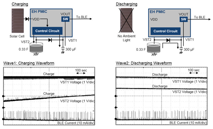
[Figure 11 | Hybrid storage control function]
Figure 12 shows the waveforms detailing the charge profile for storing energy into VSTORE2. The S6AE10xA stores energy to both VSTORE1 (small capacitor) and VSTORE2 (large capacitor). The energy is stored into VSTORE1 to operate the system and any remaining energy is used to recharge the sub storage device on VSTORE2 (VST2). The energy in VSTORE2 is supplied to the system continuously so that system can continue to operate for some time even when there is no ambient light.
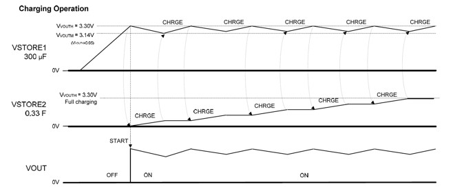
[Figure 12 | Waveform illustrating surplus energy storage]
The block diagram in Figure 13 shows hybrid power input control. Wave1 shows how the PMIC controls two power sources (solar and battery). The PMIC converts the two power sources to operate a system under various conditions. An ambient light source is generally constant, but some locations will not have constant light. The PMIC can convert two power sources automatically and continues to supply energy without ambient light.
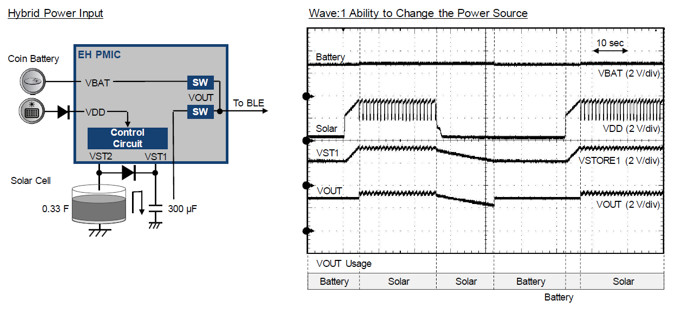
[Figure 13 | Hybrid power input control]
The S6AE10xA automatically change the power source according to the voltage level of VSTORE1. If the VSOTRE1 voltage reaches VVOUTL, energy is suppled from the VBAT power source to supply energy without ambient light.
Following are examples for how to address different operation profiles.
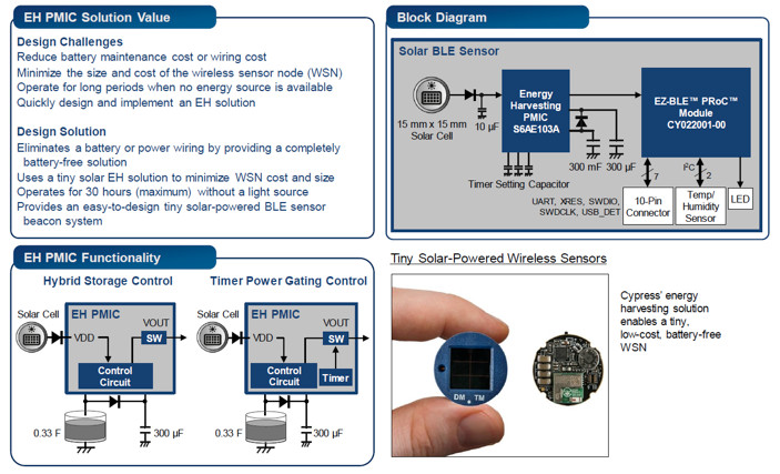
[Figure 14 | Tiny solar-powered wireless sensors needing to operate for an entire day]
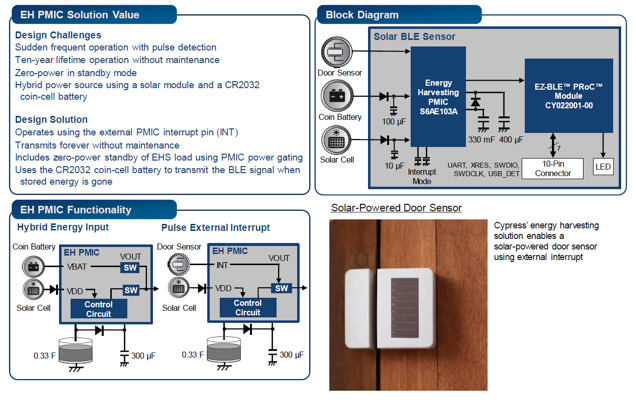
[Figure 15 | Solar-powered door sensor with sudden/frequent operation]
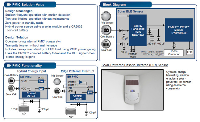
[Figure 16 | Solar-powered passive infrared sensor]


