Using a 16-bit DAC to generate a cost-efficient 18-bit DAC transfer function
November 29, 2016
High-resolution precision digital-to-analog converters (DACs) are becoming increasingly popular in modern day industrial test and measurement equipmen...
High-resolution precision digital-to-analog converters (DACs) are becoming increasingly popular in modern day industrial test and measurement equipment. In order to reduce total system cost, designers often must sacrifice resolution. The following proposes a method for building an 18-bit DAC using a 16-bit DAC and two operational amplifiers (op amps). Two different circuit topologies are analyzed that can be used to achieve the desired 18-bit output: one using a single-channel 16-bit DAC, and the other using a quad-channel 16-bit DAC. Finally, the general operating theory of both topologies is discussed, and a calibration algorithm presented. By leveraging a microcontroller with an integrated analog-to-digital converter (ADC), the algorithm achieves low differential nonlinearity (DNL) and guarantees monotonicity throughout the transfer function for less than half the cost of most precision 18-bit DACs available today.
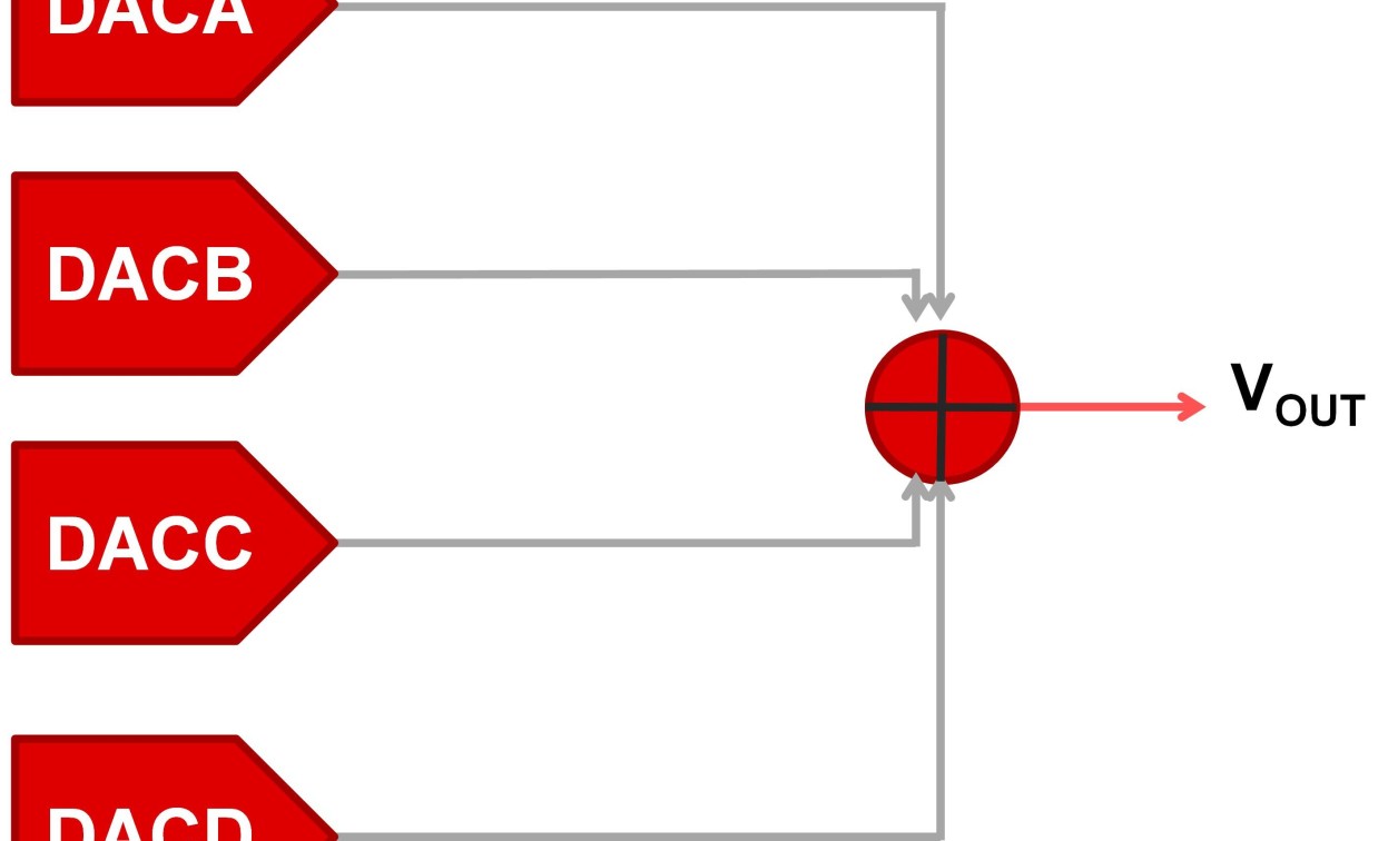
The high-level idea behind the design of a 16-bit DAC capable of producing 18-bit resolution stems from the fact that an 18-bit output can be generated by summing the output of four 16-bit DACs. Consider the block diagram in Figure 1 with the ideal transfer function.


[Figure 1 | Block diagram of a quad-channel 16-bit DAC output (top) and an ideal 18-bit DAC transfer function (bottom).]
If each 16-bit DAC has a voltage output range of 0 to 2.5 V, then DAC A can control the output from 0 to 2.5 V. While DAC A is still outputting its full-scale voltage of 2.5 V, DAC B can begin to output 0 to 2.5 V to its leg of a summing amplifier, making the output voltage of the summing amplifier 2.5 V to 5 V. This logic follows for DAC C and DAC D for the output ranges of 5 V to 7.5 V and 7.5 V to 10 V, respectively. In reality, each DAC will have a zero code error and a full-scale error region that affects the linearity of the overall transfer function (Figure 2). Now, relatively simple calibration can eliminate nonlinearities at the stitch points caused by zero code and full-scale errors.

[Figure 2 | 18-bit DAC transfer function with zero code and full-scale errors.]
Proposed circuit topologies
The obvious solution when trying to achieve this transfer function involves using a quad-channel DAC where each DAC is an input of a summing amplifier (Figure 3).

[Figure 3 | Example of a quad-channel, 16-bit DAC topology.]
The summing amplifier has the following transfer function, when:
R1=R2=R3=R4 (Equation 1)
Vout=R6R7+VDAC14+VDAC24+VDAC34+VDAC44 (Equation 2)
This topology has a lower number of devices because it uses only two integrated circuits (ICs), plus this topology has relatively simple control logic and requires only one serial peripheral interface (SPI) bus to control all four DAC channels. However, each DAC channel has a different gain error, offset error, and full-scale error, which increases the system’s overall integral nonlinearity (INL) (Figure 4a). However, the system can be calibrated such that the DACs only operate in their linear region, reducing the INL of the overall transfer function (Figure 4b) This calibration must be performed at each stitch point to achieve maximum performance because each DAC will have a different zero code error and full-scale error.


[Figure 4 | Quad-channel DAC topology transfer function (a, top) and a quad-channel DAC topology calibrated transfer function (b, bottom).]
A second topology was designed to achieve an 18-bit transfer function from 0 to 10 V after it was realized that only one DAC’s code changes at a time. Therefore, to have the desired output, the output voltage of that DAC must be summed up with 0 V, 2.5 V, 5 V, or 7.5 V. Rather than having a network of DACs create these set points, the 2.5 V reference output of the single DAC can be fed through a variable gain amplifier network, which is summed to the output of the DAC by using a summing amplifier similar to the variable reference topology (Figure 5).

[Figure 5 | Example of a variable reference topology.]
The variable reference topology has some key advantages when compared to the quad-channel DAC approach. First, since there is only one DAC, the gain and offset errors will be the same throughout the entire 18-bit transfer function, which translates into better INL than the quad-channel topology. In this variable reference topology, the stitch points pose a slightly different problem than the quad-channel DAC topology. Since the zero code error of each DAC is summed in the quad-channel topology, the stitch points have low differential linearity (DNL). However, in the variable reference topology the zero code error and offset error will cause the DNL to shift as shown in Figure 6a.


[Figure 6 | Variable reference topology transfer function (a, top), and variable reference topology calibrated transfer function (b, bottom).]
Figure 6b illustrates the results of an algorithm used to calibrate the system, and the details of that calibration are discussed next (Note that if the DAC is calibrated to operate only in its linear region, the overall system will not output a full 10 V; rather, simulations suggest the full-scale output will be approximately 9.88 V).
While the variable reference topology has a higher number of devices per board than the quad-channel DAC topology, the variable reference has a lower cost per board due to the cost savings associated with using a single-channel versus a quad-channel DAC.
Variable reference topology
The transient simulations throughout this article illustrate the benefits of calibrating the system such that the DACs only operate in their respective linear regions. Most DAC data sheets give the specification for relative accuracy (also known as INL) through codes 485d and 64714d, or 0 x 01E5 and 0 x FCCA, which is typically the DAC’s most linear operating region. To increase the total number of codes available in the overall system, 0 x FCFF is still in a fairly accurate operating region, so this will be the maximum code used in this example.
In an ideal DAC, the output voltage at code 0 x FCFF is approximately 2.4707 V. For this reason, the reference of the variable reference topology is passed through a resistor divider, which reduces the voltage to 2.46 V. If the switch is closed such that the 2.46 V reference is summed with the output of the DAC and the DAC’s code is set to 0 x 0119 (or approximately 0.0107 V) then the DNL of this step should be less than or equal to 1 least significant bit (LSB). The logic follows for the stitch points at approximately 5 V and 7.5 V as well.
Of course, the real world DAC may have an error in either the positive or negative direction at these points. Therefore, if the DNL is still unacceptable, you can use Equation 3 to find a new estimated calibration code. Gain is the gain of the variable reference circuit that will generate the next voltage range, and MAX refers to the maximum code used to set the max voltage output of the DAC (in this case 0 x FCFF).
Calibration Code= (CDACMAX+2.46 V*Gain-1)-(2.46 V*Gain)2.5 V216 (Equation 3)
Note that Equation 3 does not take gain error into account when calculating the calibration code. For this reason, the DNL may be larger than 1 LSB. If this is the case, the estimated DNL can be calculated by using Equation 4, then subtracting the DNL from the original estimated calibration code to obtain a new calibration code. This process may need to be repeated depending on the acceptable DNL of the design.
DNL= (VDACCalibration Code+{2.46 V*Gain})-(VDACMAX+2.46 V*Gain-1)2.5 V216 (Equation 4)
Assuming the system has a microcontroller with an integrated ADC to control the SPI bus and switches, the on-board ADC can be leveraged so that the microcontroller can automatically calibrate the system.
Conclusion
The two topologies discussed allow designers to generate an 18-bit transfer function from 0 to 10 V using more cost-effective 16-bit DACs, while still maintaining a low DNL at each stitch point and monotonicity throughout the range of codes.
Kunal Gandhi is a Product Marketing Engineer in the Precision Digital-to-Analog Converters group at Texas Instruments.
Texas Instruments
LinkedIn: www.linkedin.com/company-beta/1397
Facebook: www.facebook.com/texasinstruments
Google+: plus.google.com/u/0/+TexasInstruments
References
1. Kay, A. and Tim Green. Analog Engineer’s Pocket Reference, Texas Instruments, 2015