
Power, cost, performance, and security demands put mid-range FPGAs on new process roadmap
June 12, 2018
Blog

While the focus in the data center is workload acceleration, systems in these other applications need a challenging combination of low power and cost without sacrificing performance and reliability.
Applications ranging from networking and cellular infrastructure to defense, commercial aviation, and industry 4.0 require significantly different features in FPGAs than is required for the data center market. While the focus in the data center is workload acceleration, systems in these other applications still need a challenging combination of low power and cost without sacrificing performance and reliability. Attention has turned to a new class of mid-range FPGAs that are purpose-built to solve these challenges, using new process technologies, device architectures, fabric designs, transceiver strategies and built-in security measures.
The choice of process technology has a particularly significant impact on the mid-range FPGA segment. The adoption of the Silicon-Oxide-Nitride-Silicon (SONOS) non-volatile (NV) process technology enables devices to deliver a significant cost and performance advantage over alternative approaches, including SRAM-based FPGAs at the same or even smaller nodes, and floating-gate NV technology at 65nm and older nodes. The cost advantage comes from the scaling factor going from 65nm to 28nm -- approximately 50 percent. The basic transistor performance advantage at the 28nm node compared to 65nm is approximately 2.5x, using an inverter propagation delay for comparison. In addition to delivering these advantages, this approach also enables valuable features including low-power modes, “instant on” capabilities, and single-event upset (SEU) immunity.
How SONOS and floating gate NV technologies work
The device is programmed when an electronic charge is transferred to the charge storage layer to create a bias affecting the NV transistor’s characteristics. In the case of a negative charge, it acts as if the metal oxide semiconductor (MOS) transistor gate has a negative bias applied, so the device will be strongly “off.” In the case of a positive charge (depletion of electrons, or additional “holes”), the gate is positively biased, so the device will be strongly “on.”
In previous flash architectures, the floating gate non-volatile device required 17.5 V with large charge pumps that consume a substantial die area. The floating gate technology uses a double-poly transistor stack with a conductive Poly-1 layer as the charge storage element, called the floating gate. The bottom oxide thickness is critical for both preventing charge loss due to defects and determining the programming voltage. A thicker bottom oxide prevents charge loss due to oxide defects but requires a higher programming voltage. To prevent charge loss due to oxide defects, FPGA products use a relatively thick bottom oxide for high reliability. They require 17.5 V to program.
The following illustration shows a detailed description of the floating gate non-volatile device.

[Figure 1 | Floating Gate Non-Volatile Transistor.]
In contrast, SONOS technology requires only 7.5 V for programming, so charge pumps can be smaller. This technology enables a smaller die size and contributes to a more cost-effective device.
The SONOS device uses a single poly transistor stack with a non-conductive Nitride dielectric layer (silicon-nitride, Si3N4) as the charge storage element. The advantage is that if a defect exists in the bottom oxide, only a very small amount of charge will be lost in proximity to the defect. Most of the stored charge stays intact where it is because the stored charge is non-mobile in the insulating Nitride layer. This allows the use of a thinner bottom oxide that can be programmed with lower programming voltages (~7.5 V) and smaller charge pumps, compared to the floating gate technology.
The following illustration shows the SONOS transistor.

[Figure 2 | SONOS technology]
Though SONOS requires some extra process steps compared to an unenhanced CMOS manufacturing process, it uses fewer transistors than an SRAM memory element, so is very cost- competitive.
Improved reliability and power efficiency
The 28nm SONOS NV technology improves reliability by using a push-pull cell containing an N-channel and a P-channel NV device. The NV devices are not in the data-speed path and are only used to control a standard transistor used as the data-path switch. This provides a large functional advantage because any variation in the NV device threshold voltage (Vt) does not change the switch conductance.
A simple description of a push-pull cell is that the N-ch and P-ch devices are stacked in a series with each other between the power and ground rails, with one in the “on state” and one in the “off state.” The N-ch and P-ch NV devices compete against each other to control the gate of the switch transistor. The On device will overpower the Off device and drive the gate of the switch device to a high or low voltage (depending on which NV transistor is on and off), thus putting the switch in either an on or off state. If either of the NV devices is a weak bit (that is, at the lowest Vt limit allowed), the other bit still holds the correct state. This acts as a built-in quasi redundancy, because one NV device can be weak and no performance degradation will occur over the life of the product.
The new generation of FPGAs also consumes much lower power compared to alternative FPGA technologies. A significant reason for this is the SONOS NV FPGA configuration cell. The following illustration shows two schematics of the NV cell, highlighting the different programmable “configuration” states that control the FPGA data signal path. There is an off state where the datapath is switched off and an on state where the datapath is switched on.
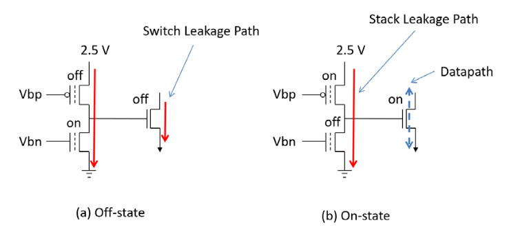
[Figure 3 | Stack and switch leakage paths.]
Consider the stack and switch leakage paths (Figure 3). In the “stack” leakage path, one of the two NV elements is always programmed into a very deep off-state condition. Using “on state” as an example, the N-ch NV element is in the off state with its Vt shifted ~0.5 V above a normal transistor Vt, consequently the leakage will go down to a negligible level. The leakage of the NV stack is extremely low—much lower than the leakage of a standard CMOS transistor stack. In addition, there are fewer transistors in an NV configuration memory cell than in an SRAM memory cell.
The “switch” leakage path is the leakage across an “off-state” switch—the “FPGA logic signal path” leakage. The switch device is a high-voltage device and has been optimized to provide much lower leakage than a standard transistor.
New capabilities
SONOS NV technology also enables several new FPGA capabilities, the first of which is a power-saving mode. An example of this capability can be seen in Microsemi’s PolarFire FPGA Flash*Freeze mode, during which the product can be put into a state that turns the supply voltage off to the configuration memories in the FPGA logic block while saving the user’s state in low-power latches. This lowers the standby power by approximately two-thirds. Microsemi’s unique implementation of this capability is enabled by the usage of the NV configuration cell that is not possible with volatile FPGA technologies. The NV cell will retain its state after power has been turned off to the device, allowing the FPGA to return to normal operation without reconfiguration.
Another important capability occurs at power-up: there is no need to reload the FPGA design code when power is returned because the FPGA logic configuration cell retains its state after power down. Thus, there is no need for an external boot PROM and the programmed FPGA is fully functional as a single chip. Also, the boot time is very fast because there is no large transfer or decryption of data that must occur before the FPGA is usable. The millions of configuration cells are directly controlling the corresponding switch transistors as soon as power is applied.
Additionally, non-volatile technology makes the FPGA logic configuration SEU-immune. This contrasts with the configuration memory in SRAM-based FPGAs, which can flip state due to neutron hits. Configuration memory upsets are especially problematic because the configuration memory must remain static and error free during all the operating hours of the device for correct FPGA operation. Any upset will be persistent until the device is powered-down or the cell is reprogrammed correctly. If an upset occurs in the erroneous state, the logic or routing of the FPGA fabric will be wrong, potentially causing not just a single wrong data value, but a string of wrong results until it is fixed. This may require a full system reboot. In the example of the PolarFire FPGA family, the SONOS NV charge is stored in the nitride dielectric, which is not susceptible to charge loss from neutron hits. This improves reliability as compared to SRAM FPGAs.
Cost-optimized mid-range FPGAs devices are increasingly important in applications that require the lowest possible power at densities up to 500K logic elements (LEs) for communications, defense, and industrial markets. Moving to SONOS NV process technology enables FPGAs to deliver a significant cost and performance advantage over alternative approaches, including SRAM-based FPGAs at the same or even smaller nodes, and floating-gate NV technology at 65nm and older nodes.


