
Over-the-Air (OTA) Updates in Embedded Microcontroller Applications: Design Trade-Offs and Lessons Learned
November 13, 2018
Story

In this article, we will describe several different software designs for OTA updates and discuss their trade-offs.
Abstract
Many embedded systems are deployed in places that are difficult or impractical for a human operator to access. This is especially true for Internet of Things (IoT) applications, which are typically deployed in larger quantities and with limited battery life. Some examples would be embedded systems that monitor the health of a person or a machine. These challenges, coupled with the rapid software lifecycle, cause many systems to require support for over-the-air (OTA) updates. An OTA update replaces the software on the microcontroller or microprocessor of the embedded system with new software. While many people are very familiar with OTA updates on their mobile devices, the design and implementation on a resource constrained system leads to many different challenges. In this article, we will describe several different software designs for OTA updates and discuss their trade-offs. We will see how hardware features of two ultra-low power microcontrollers can be leveraged in an OTA update software.
Building Blocks
Server and Client
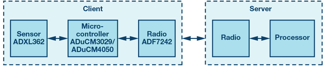
An OTA update replaces the current software on a device with new software, with the new software being downloaded wirelessly. In an embedded system, the device that runs this software is typically a microcontroller. A microcontroller is a small computing device with limited memory, speed, and power consumption. A microcontroller typically contains a microprocessor (core) as well as digital hardware blocks for specific operations (peripherals). Ultra-low power microcontrollers that typically consume 30 μA/MHz to 40 μA/MHz in active mode are ideal for this type of application. Using specific hardware peripherals on these microcontrollers and placing them into low power modes is an important part of the OTA update software design. An example of an embedded system that might require OTA updates is shown in Figure 1. Here we see a microcontroller connected with a radio and sensor, which may be used in an IoT application that gathers data about the environment using the sensor and reports it periodically using the radio. This portion of the system is referred to as the edge node or client and is the target of the OTA update. The other portion of the system is referred to as the cloud or server and is the provider of the new software. The server and client communicate over a wireless connection using transceivers (radios).
What Makes a Software Application?
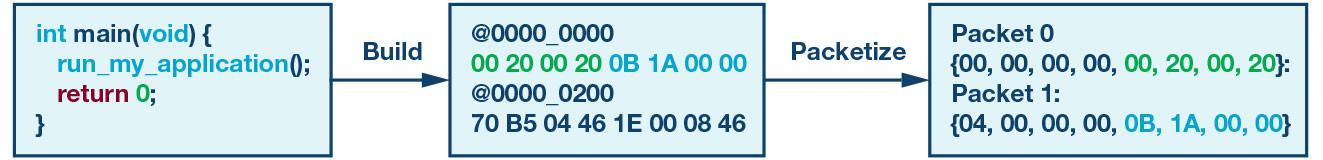
Much of the OTA update process is the act of transferring the new software from the server to the client. The software is transferred as a sequence of bytes, after it has been converted into a binary format from the source format. The conversion process compiles the source code files (for example, c, cpp), links them together into an executable file (for example, exe, elf), and then the executable is converted into a portable binary file format (for example, bin, hex). At a high level, these file formats contain a sequence of bytes that belong at a specific address of memory in the microcontroller. Typically, we conceptualize the information being sent over a wireless link as data, such as a command to change the system’s state or sensor data collected by the system. In the case of the OTA update, the data is the new software in binary format. In many cases, the binary file will be too large to send in a single transfer from the server to the client, meaning that the binary file will need to be placed into separate packets, in a process called packetizing. To visualize this process better, Figure 2 demonstrates how different versions of the software will produce different binary files, and thus different packets to be sent during the OTA update. In this simple example, each packet contains 8 bytes of data, with the first 4 bytes representing the address in the client’s memory to store the next 4 bytes.
Major Challenges
Based on this high-level description of the OTA update process, three major challenges arise that the OTA update solution must address. The first challenge relates to memory. The software solution must organize the new software application into volatile or nonvolatile memory of the client device so that it can be executed when the update process completes. The solution must ensure that a previous version of the software is kept as a fallback application in case the new software has problems. Also, we must retain the state of the client device between resets and power cycles, such as the version of the software we are currently running, and where it is in memory. The second major challenge is communication. The new software must be sent from the server to the client in discrete packets, each targeting a specific address in the client’s memory. The scheme for packetizing, the packet structure, and the protocol used to transfer the data must all be accounted for in the software design. The final major challenge is security. With the new software being sent wirelessly from the server to the client, we must ensure that the server is a trusted party. This security challenge is known as authentication. We also must ensure that the new software is obfuscated to any observers, since it may contain sensitive information. This security challenge is known as confidentiality. The final element of security is integrity, ensuring that the new software is not corrupted when it is sent over the air.
The Second-Stage Boot Loader (SSBL)
Understanding the Boot Sequence
The primary boot loader is a software application that permanently resides on the microcontroller in read-only memory. The region of memory the primary boot loader resides in is known as info space and is sometimes not accessible to users. This application executes every time a reset occurs, generally performing some essential hardware initializations, and may load user software into memory. However, if the microcontroller contains on-chip nonvolatile memory, like flash memory, the boot loader does not need to do any loading and simply transfers control to the program in flash memory. If the primary boot loader does not have any support for OTA updates, it is necessary to have a second-stage boot loader. Like the primary boot loader, the SSBL will run every time a reset occurs, but will implement a portion of the OTA update process. This boot sequence is illustrated in Figure 3. In this section, we will describe why a second-stage boot loader is necessary and how specifying the role of this application is a key design trade-off.

Lesson Learned: Always Have an SSBL
Conceptually, it may seem simpler to omit the SSBL and place all the OTA update functionality into the user application, as it would allow an existing software framework, operating system, and device drivers to be seamlessly leveraged for the OTA process. The memory map and boot sequence of a system that chose this approach is illustrated in Figure 4.

Application A is the original application that is deployed on the microcontroller in the field. This application contains the OTA update-related software, which is leveraged to download Application B when requested by the server. After this download is complete and Application B has been verified, Application A will transfer control to Application B by performing a branch instruction to the reset handler of Application B. The reset handler is a small piece of code that is the entry point of the software application and runs on reset. In this case, the reset is mimicked by performing a branch, which is equivalent to a function call. There are two major issues with this approach:
- Many embedded software applications employ a real-time operating system (RTOS), which allows the software to be split into concurrent tasks, each with different responsibilities in the system. For instance, the application presented in Figure 1 may have RTOS tasks for reading the sensor, running an algorithm on the sensor data, and interfacing with the radio. The RTOS itself is always active and is responsible for switching between these tasks based on asynchronous events or specific time-based delays. As a result, it is not safe to branch to a new program from an RTOS task, since other tasks will remain running in the background. The only safe way to terminate a program with a real-time operating system is through a reset.
- Based on Figure 4, a solution to the previous issue would be to have the primary boot loader branch to Application B instead of Application A. However, on some microcontrollers, the primary boot loader always runs the program that has its interrupt vector table (IVT), a key portion of the application that describes interrupt handling functions, located at address 0. This means that some form of IVT relocation is necessary to have a reset map to Application B. If a power cycle occurs during this IVT relocation, it could leave the system in a permanently broken state.
These issues are mitigated by having an SSBL fixed at address 0, as illustrated in Figure 3. Since the SSBL is a non-RTOS program, it can safely branch to a new application. There is no concern of a power cycle placing the system in a catastrophic state since the IVT of the SSBL at address 0 is never relocated.
Design Trade-Off: The Role of the SSBL
We’ve spent a lot of time discussing the SSBL and the relationship it has with the application software, but what does this SSBL program do? At the bare minimum, the program must determine what the current application is (where it begins) and then branch to that address. The location of the various applications in the microcontroller memory is generally kept in a table of contents (ToC) as shown in Figure 3. This is a shared region of persistent memory that both the SSBL and application software use to communicate with each other. When the OTA update process completes, the ToC is updated with the new application information. Portions of the OTA update functionality can also be pushed to the SSBL. Deciding what portions is an important design decision when developing OTA update software. The minimal SSBL described above will be extremely simple, easy to verify, and most likely will not require modifications during the life of the application. However, this means that each application must be responsible for downloading and verifying the next application. This can lead to code duplication in terms of the radio stack, device firmware, and OTA update software. On the other hand, we can choose to push the entire OTA update process to the SSBL. In this scenario, applications simply set a flag in the ToC to request an update and then perform a reset. The SSBL then performs the download sequence and verification process. This will minimize code duplication and simplify the application specific software. However, this introduces a new challenge of potentially having to update the SSBL itself (that is, updating the update code). In the end, deciding what functionality to place in the SSBL will depend on the memory constraints of the client device, the similarity between downloaded applications, and the portability of the OTA update software.
Design Trade-Off: Caching and Compression
Another key design decision in the OTA update software will be how to organize the incoming application in memory during the OTA update process. The two types of memory that are typically found on a microcontroller are nonvolatile memory (for example, flash memory) and volatile memory (for example, SRAM). The flash memory will be used to store the program code and read-only data of an application, along with other system-level data such as the ToC and an event log. The SRAM will be used to store modifiable portions of the software application, such as nonconstant global variables and the stack. The software application binary illustrated in Figure 2 only contains the portion of the program that lives in nonvolatile memory. The application will initialize the portions that belong in volatile memory during a startup routine.
During the OTA update process, every time the client device receives a packet from the server containing a portion of the binary it will be stored in SRAM. This packet could be either compressed or uncompressed. The benefit of compressing the application binary is that it will be smaller in size, allowing for fewer packets to be sent and less space needed in SRAM to store them during the download procedure. The disadvantage of this approach is the extra processing time that the compression and decompression add to the update process, along with having to bundle compression related code in the OTA update software.
Since the new application software belongs in flash memory but arrives into SRAM during the update process, the OTA update software will need to perform a write to flash memory at some point during the update process. Temporarily storing the new application in SRAM is called caching. At a high level, there are three different approaches the OTA update software could take to caching.
- No caching: Every time a packet arrives containing a portion of the new application, write it to its destination in flash memory. This scheme is extremely simple and will minimize the amount of logic in the OTA update software, but it requires that the region of flash memory for the new application is fully erased. This method wears down the flash memory and adds overhead.
- Partial caching: Reserve a region of SRAM for caching, and when new packets arrive store them in that region. When the region fills up, empty it by writing the data to flash memory. This can get complex if packets arrive out of order or there are gaps in the new application binary, since a method of mapping SRAM addresses to flash addresses is required. One strategy is to have the cache act as a mirror of a portion of flash memory. Flash memory is divided into small regions known as pages, which are the smallest division for erasing. Because of this natural division, a good approach is to cache one page of flash memory in SRAM and when it fills up or the next packet belongs in a different page, flush the cache by writing that page flash memory.
- Full caching: Store the entire new application in SRAM during the OTA update process and only write it to flash memory when it has been fully downloaded from the server. This approach overcomes the shortcomings of the previous approaches by minimizing the number of writes to flash memory and avoiding complex caching logic in the OTA update software. However, this will place a limit on the size of the new application being downloaded, since the amount of available SRAM on the system is typically much smaller than the amount of available flash memory.
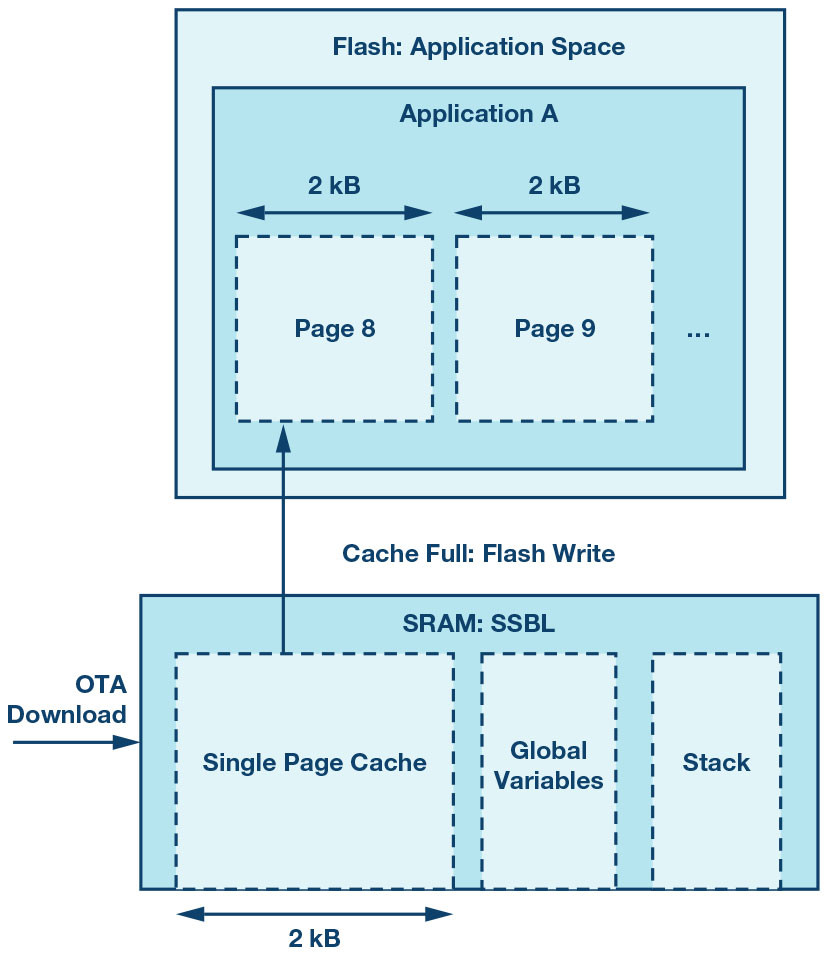
The second scheme of partial caching during an OTA update is illustrated in Figure 5, where the portion of flash memory for Application A from Figures 3 and 4 is magnified and a functional memory map of the SRAM for the SSBL is illustrated. An example flash page size of 2 kB is shown. Ultimately this design decision will be determined based on the size of the new application and the allowed complexity of the OTA update software.
Security and Communication
Design Trade-Off: Software vs. Protocol
The OTA update solution must also address security and communication. Many systems like the one shown in Figure 1 will have a communication protocol implemented in hardware and software for normal (non-OTA update related) system behavior like exchanging sensor data. This means that there is a method of (possibly secure) wireless communication already established between the server and the client. Communication protocols that an embedded system like Figure 1 might use would be, for example, Bluetooth Low Energy (BLE) or 6LoWPAN. Sometimes these protocols have support for security and data exchange that the OTA update software may be able to leverage during the OTA update process.
The amount of communication functionality that must be built into the OTA update software will ultimately be determined by how much abstraction is provided by the existing communication protocol. The existing communication protocol has facilities for sending and receiving files between the server and client that the OTA update software can simply leverage for the download process. However, if the communication protocol is more primitive and only has facilities for sending raw data, the OTA update software may need to perform packetizing and provide metadata along with the new application binary. This also applies to the security challenges. The onus may be on the OTA update software to decrypt the bytes being sent over the air for confidentiality if the communication protocol does not support this.
In conclusion, building facilities like custom packet structure, server/client synchronization, encryption, and key exchange into the OTA update software will be determined based on what the system’s communication protocol provides and what the requirements are for security and robustness. In the next section, we will propose a complete security solution that solves all the challenges introduced earlier and we will show how to leverage a microcontroller’s cryptographic hardware peripheral in this solution.
Solving Security Challenges
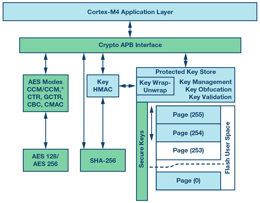
Our security solution needs to keep the new application sent over-the-air confidential, detect any corruption in the new application, and verify that the new application was sent from a trusted server as opposed to a malicious party. These challenges can be solved using cryptographic (crypto) operations. Specifically, two cryptographic operations known as encryption and hashing can be used in the security solution. Encryption will use a shared key (password) between the client and server to obfuscate the data being sent wirelessly. A specific type of encryption that the microcontroller’s crypto hardware accelerator may support is called AES-128 or AES-256, depending on the key size. Along with the encrypted data, the server can send a digest to ensure that there is no corruption. The digest is generated by hashing the data packet—an irreversible mathematical function that generates a unique code. If any part of the message or digest is modified after the server creates them, like a bit being flipped during wireless communication, the client will notice this modification when it performs the same hash function on the data packet and compares the digests. A specific type of hashing that the microcontroller’s crypto hardware accelerator may support is SHA-256. Figure 6 shows a block diagram of a crypto hardware peripheral in the microcontroller, with the OTA update software residing in the Cortex-M4 application layer. This figure also shows the support for protected key storage in the peripheral, which can be leveraged in the OTA update software solution to safely store the client’s keys.
A common technique to solve the final challenge of authentication is to use asymmetric encryption. For this operation, the server generates a public-private key pair. The private key is known only by the server and the public key is known by the client. Using the private key, the server can generate a signature of a given block of data—like the digest of the packet that will be sent over the air. The signature is sent to the client, who can verify the signature using the public key. This enables the client to confirm the message was sent from the server and not a rogue third party. This sequence is illustrated in Figure 7, with solid arrows representing function input/output and dashed arrows showing the information that is sent over the air.
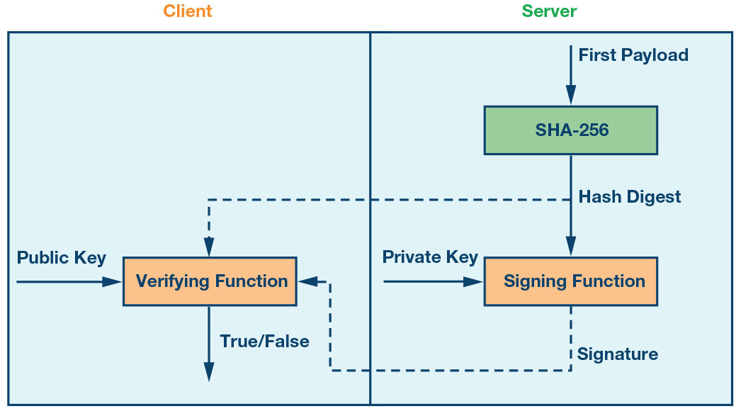
Most microcontrollers do not have hardware accelerators for these asymmetric encryption operations, but they can be implemented using software libraries such as Micro-ECC, which specifically targets resource constrained devices. The library requires a user-defined random number generating function, which can be implemented using the true random number generator hardware peripheral on the microcontroller. While these asymmetric encryption operations solve the trust challenge during an OTA update, they are costly in terms of processing time and require a signature to be sent with the data, which increases packet sizes. We could perform this check once at the end of the download, using a digest of the final packet or the digest of the entire new software application, but that would allow third parties to download untrusted software to the client, which is not ideal. Ideally, we want to verify every packet that we receive is from our trusted server without the overhead of a signature each time. This can be achieved using a hash chain.
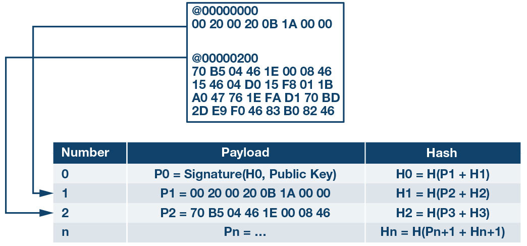
A hash chain incorporates the cryptographic concepts we have discussed in this section into a series of packets to tie them together mathematically. As Figure 8 shows, the first packet (number 0) contains the digest of the next packet. Instead of the actual software application data, the payload of the first packet is the signature. The second packet (number 1) payload contains a portion of the binary, and the digest of the third packet (number 2). The client verifies the signature in the first packet and caches the digest, H0, for later use. When the second packet arrives, the client hashes the payload and compares it to H0. If they match, the client can be sure that this subsequent packet was from the trusted server without all the overhead of doing a signature check. The expensive task of generating this chain is left to the server, and the client must simply cache and hash as each packet arrives to ensure packets arrive uncorrupted, with integrity, and authenticated.
Experimental Setup
The ultra-low power microcontrollers that solve the memory, communication, and security design challenges mentioned in this article are the ADuCM3029 and ADuCM4050. These microcontrollers contain the hardware peripherals discussed for OTA updates such as flash memory, SRAM, crypto accelerator, and a true random number generator. The device family packs (DFPs) for these microcontrollers provide software support for building an OTA update solution on these devices. The DFP contains peripheral drivers that provide simple, flexible interfaces for using the hardware.
Hardware Configuration
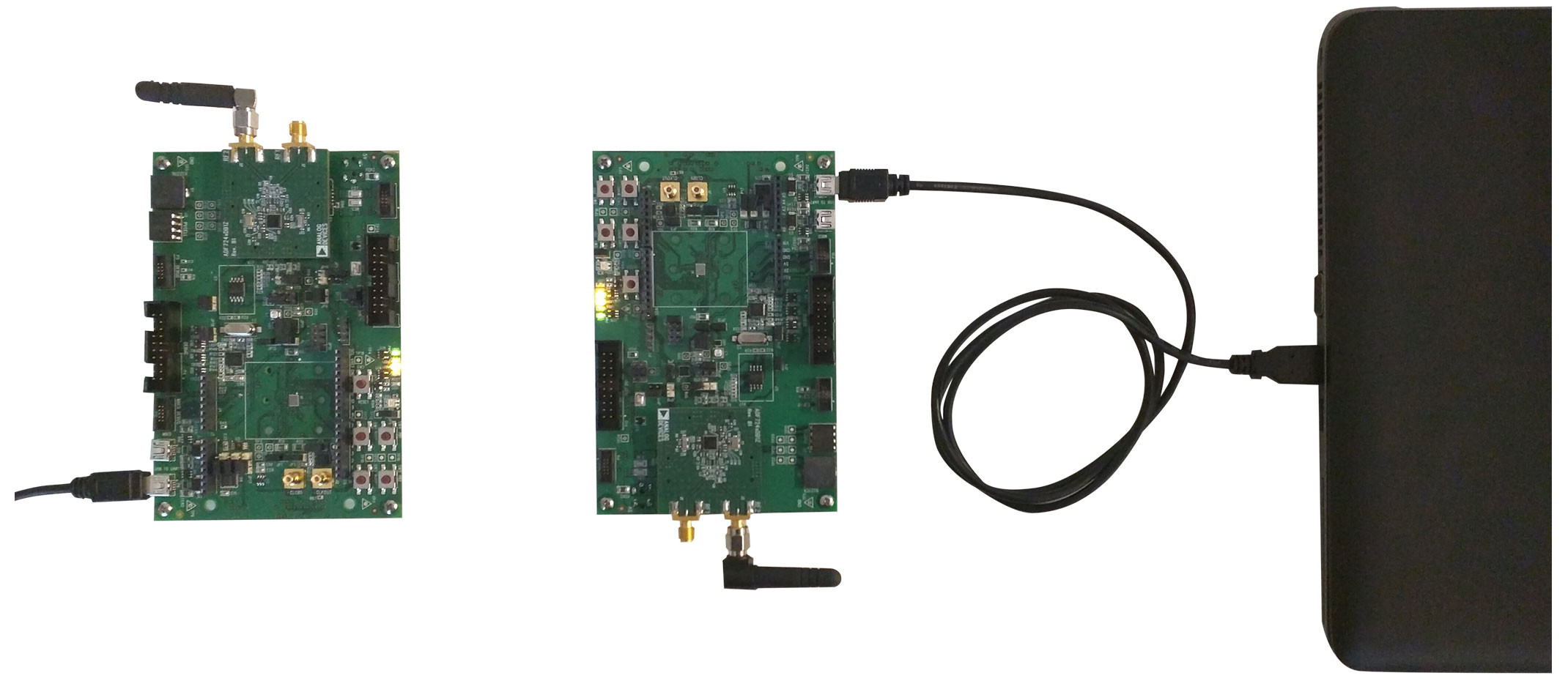
To verify and validate the concepts discussed here, an OTA update software reference design was created using the ADuCM4050. For the client, an ADuCM4050 EZ-KIT is connected to an ADF7242 using the transceiver daughter board horseshoe connector. The client device is pictured on the left of Figure 9. For the server, a Python application was developed that runs on a Windows PC. The Python application communicates over the serial port to another ADuCM4050 EZ-KIT that also has an ADF7242 attached in the same arrangement as the client. However, the right EZ-KIT in Figure 9 performs no OTA update logic, and simply relays packets received from the ADF7242 to the Python application.
Software Components
The software reference design partitions the flash memory of the client device as shown in Figure 3. The main client application was designed to be very portable and configurable such that it could be leveraged in other arrangements or on other hardware platforms. Figure 10 shows the software architecture of the client device. Note that while we sometimes refer to this entire application as the SSBL, in Figure 10 and from now on we logically separate the true SSBL portion (in blue) from the OTA update portion (in red), as the latter is not necessarily required to be implemented entirely in the same application as previously discussed. The hardware abstraction layer shown in Figure 10 keeps the OTA client software portable and independent of any underlying libraries (shown in orange).

The software application implements the boot sequence in Figure 3, a simple communication protocol for downloading the new application from the server, and the hash chain. Each packet in the communication protocol has a 12-byte metadata header, 64-byte payload, and a 32-byte digest. In addition, it has the following features:
- Caching: Support for both no caching or caching one page of flash memory, depending on user configuration.
- Table of Contents: The ToC is designed to only hold two applications, and the new application is always downloaded into the oldest spot, to keep a fallback application. This is called an A/B update scheme.
- Messaging: Support for either the ADF7242 or UART for messaging, depending on user configuration. Using the UART for messaging eliminates the left EZ-KIT in Figure 9, leaving the kit on the right for the client. This over-the-wire update scheme is useful for initial system bring-up and debugging.
Results
Along with meeting the functional requirements and passing a variety of tests, the performance of the software is also critical to determining project success. Two metrics that are commonly used to measure the performance of embedded software are footprint and cycles. Footprint refers to how much space the software application takes up in volatile (SRAM) and nonvolatile (flash) memory. Cycles refers to the number of microprocessor clock cycles the software uses to perform a specific task. While being similar to software run-time, it accounts for the fact that the software may enter low power modes while performing the OTA update where the microprocessor is inactive, and no cycles are consumed. While the software reference design was not optimized for either of these metrics, they are useful for benchmarking the program and comparing design trade-offs.
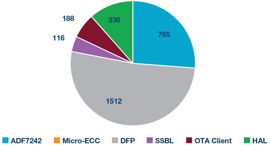
Figure 11 and Figure 12 show the footprint of the OTA updates software reference design implemented on the ADuCM4050 with no caching. The figures are partitioned according to the components illustrated in Figure 10. As Figure 11 shows, the entire application uses around 15 kB of flash memory. This is quite small considering the ADuCM4050 contains 512 kB of flash memory. The true application software (the software developed for the OTA update process) only takes about 1.5 kB, with the rest being used for libraries such as the DFP, Micro-ECC, and ADF7242 stack. These results help to illustrate the design trade-off of what role the SSBL should have in the system. The majority of the 15 kB footprint is for the update process. The SSBL itself only takes around 500 bytes of footprint, with an additional 1 kB to 2 kB of DFP code for device access like the flash driver.

To evaluate the overhead of the software, we perform cycle counting every time a data packet is received and then look at the average number of cycles consumed per packet. Each data packet requires AES-128 decryption, SHA-256 hashing, a write to flash memory, and some packet metadata validation. With a packet payload size of 64 bytes and no caching, the overhead is 7409 cycles to process a single data packet. Using a 26 MHz core clock, this is about 285 microseconds of processing time. The value was calculated using the cycle counting driver located in the ADuCM4050 DFP (unadjusted cycles) and is the average taken during a 100 kB binary download (about 1500 packets). The minimal overhead per packet can be attributed to the drivers in the DFP leveraging the direct memory access (DMA) hardware peripheral on the ADuCM4050 when performing bus transactions and the drivers placing the processor into a low power sleep state during each transaction. If we disable the use of low power sleeping in the DFP and change the bus transactions to not use DMA, the overhead per data packet increases to 17,297 cycles. This illustrates the impact that efficient use of device drivers has on an embedded software application. While the overhead is also kept low by having a small number of data bytes per packet, doubling the data bytes per packet to 128 only yields a small increase in cycles—resulting in 8,362 cycles for the same experiment.
Cycles and footprint also illustrate the trade-off discussed earlier of caching packet data instead of writing to flash memory each time. With one page of flash memory caching enabled, the overhead per data packet reduces from 7,409 to 5,904 cycles. This 20 percent reduction comes from the ability to skip the flash write for most packets and only perform a flash write when the cache is full. The reduction comes at a price of SRAM footprint. Without caching, the HAL only requires 336 bytes of SRAM, as shown in Figure 12. However, when caching is used we must reserve space equal to a full page of flash memory, which increases the SRAM utilization to 2,388 bytes. The flash memory utilization of the HAL also increases by a small amount due to the extra code needed to determine when the cache must be flushed.
These results demonstrate the tangible impact the design decisions will have on the performance of the software. There is no one-size-fits-all solution—each system will have different requirements and constraints, and the OTA update software will need to be tuned to address them. Hopefully this article has shed some light on common problems and trade-offs that were faced when designing, implementing, and validating an OTA update software solution.
References
Nilsson, Dennis Kengo and Ulf E. Larson. “Secure Firmware Updates over the Air in Intelligent Vehicles.” ICC Workshops—2008 IEEE International Conference on Communications Workshops, May 2008.
About the Author
Benjamin Bucklin Brown ([email protected]) joined Analog Devices in 2016 after graduating from McGill University with a Bachelor of Engineering in electrical engineering. Currently he works as an embedded software engineer in the Consumer Sensing and Processing Technology (CSPT) Group, developing firmware for application-specific integrated circuits. Previously, he worked in the IoT Platform Technology Group, developing device drivers and software reference applications for the ADuCM3029 and ADuCM4050 microcontrollers.


