
How to build a PCIe/104 system
October 20, 2016
Story
In 2008 the ever prominent PC/104 Consortium injected fresh life into their long established PC/104 stackable format; foreseeing the industry decline...
In 2008 the ever prominent PC/104 Consortium injected fresh life into their long established PC/104 stackable format; foreseeing the industry decline in PCI bus derived peripheral components in favour of the ‘new kid on the block’ PCI Express – enter the PCIe/104. Unlike its predecessors, ISA and PCI, PCI Express is actually not a bus in the traditional sense, but a collection of links from a single host to a single device.
As we’re not comparing ‘spades with spades’, some background terminology must first be explained. PCI Express employs lanes and links; the former a transmit differential pair and receive differential pair connection between two devices, the latter comprising of one (or more) lanes and a clock differential pair. Links are labelled as xY, where Y defines quantity of pairs of transmit/receive lanes, always with a single clock differential pair. Crudely x4 offers quadruple bandwidth of x1 and so forth.
This all starts to sound complex, especially against the backdrop of the perception that assembling historic ISA and PCI derived PC/104 stacks was effortless (often not entirely true) as our memories often omit any niggles and nuances. PCIe/104 is designed to shield the integrator from low-level compatibility considerations, making it easy to configure a system by automatic link shifting so there are no switches or jumpers to set, ever. Simplistically there’s typically very little ‘how to’ in PCIe/104 – just build your stack!

Link shifting
It’s easy to become overwhelmed with the terminology of the underlying configuration, but the key ‘take-away’ is one need not concern themselves with the intricacies, PCIe/104 self-configures. That said, engineers naturally have an unquenchable thirst to understand what happens underneath that proverbial bonnet, so here goes. For simplicity we’ll focus on a single link (x1) scenario but x4, alongside SATA, USB 2.0 and 3.0 all operate identically.
Link shifting functions by assigning each peripheral board the first link presented to it, then shifting the remaining links so the next peripheral card in the stack has an active link in the first position. Below (Figure 1) we see a simplified host with four PCIe links going up. The peripheral card installed directly above a host uses link 1 coming in from the bottom connector and then shifts link 2 from the bottom to link 1 on the top, shifts link 3 from the bottom to link 2 on the top, and finally shifts link 4 from the bottom to link 3 on the top.

Figure 1. Link shifting operates by having each peripheral board use the first PCI Express lane presented to it and shifting the remaining links so the next card in the stack will have an active link in the first position. Shown here is a simplified host with four PCI Express links.
This continues as additional PCIe peripheral cards are added to the stack, until all four links are utilised via link shifting as demonstrated below in Figure 2.
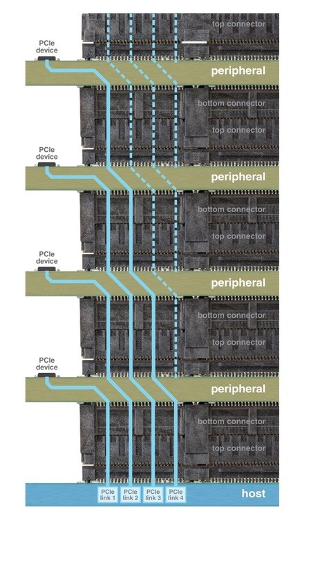
Figure 2: Four PCIe/104 x1 Peripheral Stack
Notice that the four peripheral boards are exactly the same yet each gets its own PCI Express link and will be recognized by the host as a separate device automatically. That’s a good foundation for examining PCIe/104 link shifting in detail. In the above example, the host CPU only has a connector on the top. If a host had the connector only on the bottom, the peripheral board would have to change because the host would be supplying PCI Express links to the peripheral’s top connector and the PCIe device on the peripheral board is expecting the PCI Express link to be coming in from the bottom connector. PCIe/104 resolved this by requiring all peripherals to add a signal switch to the board that is controlled by a direction signal. The direction signal informs the peripheral whether it is installed above or below the host so it can select a link from the top or bottom connector automatically depending on its location.
In the example below, the host CPU actually has eight PCI Express x1 links and sends four up the stack and four separate links down the stack. This means that peripherals can be stacked both above and below the CPU at the same time. In this example only links 1, 6, 7 and 8 are used, leaving links for three more devices above and one below the host. A close inspection of the peripheral boards above and below the host shows them to be identical. This means that a peripheral will work in any location in the stack, making things really easy for system designers.
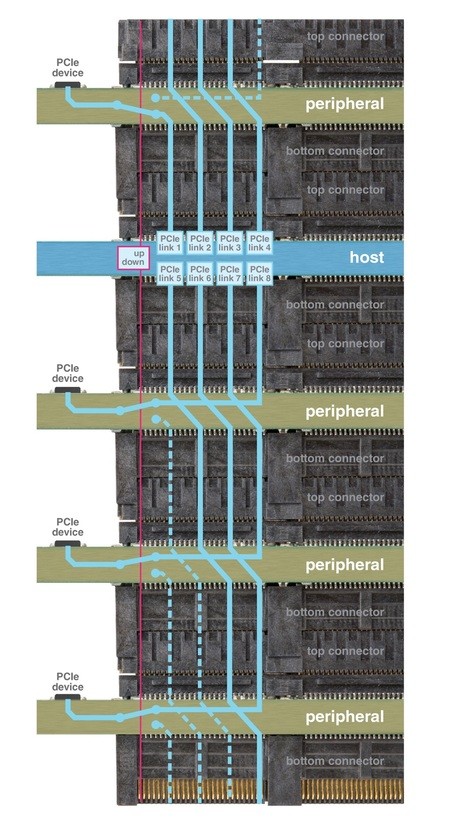
Figure 3: Host CPU module providing top and bottom peripheral stacking
PCIe/104 link shifting simplifies system configuration and provides maximum flexibility for users. Hosts can allow stack up, stack down, or both at the same time and know that any peripheral will work. Also, peripheral manufacturers only have to build one version of a device and know that it will work above or below any host.
Stacking Rules
The PCIe/104 specification defines four stacking rules.
- Peripheral modules connecting with PCI Express x1 or x4 links, USB 2.0 links, or SMB are universal and can plug into either a Type 1 or a Type 2 host.
- Peripheral modules connecting with PCI Express x16 or x8 links must plug into a Type 1 host.
- Peripheral modules connecting with SATA, USB 3.0, or LPC links must plug into a Type 2 host.
- Any peripheral module plugged in the wrong bus holds the system in reset and causes no damage.
All of the above applies to SATA and USB. The only additional concerns when stacking multiple device types is stacking order. PCIe/104 has some simple rules to ensure this is easy. The general rule is to build a stack by putting higher clock rate peripherals closer to the host. Follow the priority below:
- Gen 3 PCI Express at 8.0 Gigabits/second closest to the host
- SATA 3 at 6.0 Gigabits/second next closest
- Gen 2 PCI Express and USB 3.0 at 5.0 Gigabits/second
- SATA 2 at 3.0 Gigabits/second
- Gen 1 PCI Express at 2.5 Gigabits/second
- PCIe/104 and PCI/104-Express Specification Revision 3.0 February 17, 2015 Page 4
- SATA 1 at 1.5 Gigabits/second
- USB 2.0 at 480 Mbits/second
OneBank Stacking
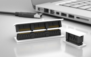
The latest addition to the PC/104 family is OneBank® which is the first bank of the standard PCIe/104 three bank connector and will work with most PCIe x1 and USB 2.0 peripherals. While it was designed to physically stack with the three bank connector, the absence of the second and third bank of the connector makes a difference in the bus functionality.
Host boards with OneBank connectors are compatible with PCIe/104 x1 and USB 2.0 peripherals and since the OneBank connector does not carry +12VDC power any boards that use +12VDC will not work with OneBank hosts.
OneBank peripheral boards that are being used with PCIe/104 hosts do not pass +12VDC, SATA, USB 3.0, PCIe x4, PCIe x8, or PCIe x16 links. Therefore, all boards using these links will need to be physically closer to the host than any OneBank boards.

Figure 4: OneBank® Stack
PCIe/104 as a Mezzanine Module
PC/104 was the original System-On-Module adopted as an open standard in March 1992 by the PC/104 Consortium; its beauty was it functioned (and still does) equally well as a true, standalone single-board-computer. System integrators can standardise on a single CPU module to benefit from quantities of scale yet deploy it on its own, within a PC/104 stack, or as the heart of a custom baseboard. CPU development has always been expensive and risky and since the very beginnings of our embedded industry the logical design approach has rarely been needlessly re-inventing the wheel. PC/104 as a mechanical form factor hoovers up almost every conceivable peripheral bus and I/O function across its almost inconceivable range, all designed to be as plug’n’play as the underlying technology (especially of yesteryear) can allow. Furthermore, even today PC/104 covers a vast performance spectrum, from ultra-low power ARM® processors to the lightning quick, quad core, Intel® Core i7. PCIe/104 brings PCI Express, USB 3.0, SATA, and LPC connectivity to the party.
The heart of any system utilising the benefits of PC/104 need not be PC/104 itself, some applications demand the processing element and complex industry specific peripheral circuitry co-exist on the same PCB. For these scenarios the balance between satisfying a wide enough function set to fit your client base vs risking superfluous functionality, driving up cost at the expense of being competitive is a notoriously difficult balance to strike. Deploying a PC/104, PCI/104 or PCIe/104 expansion bus onto your bespoke design means your ability to expand the system just became limitless – all without impact on your design’s standard unit price.
The legacy continues…
PC/104 has been used for over 25 years in myriad rugged MIL/COTS applications, spanning almost every conceivable industry and using countless operating systems. PCIe/104 was added in 2008 to allow these applications to expand their capability and performance by employing high speed PCI Express. This introduced the first surface mount peripheral ‘bus’ connectors and PCI Express link shifting makes a point-to-point bus work in a stacking architecture in a manner designed to simplify system configuration. PCIe/104’s inherent ruggedness and broad supplier base using the open standards continues to make the PC/104 form factor an ideal platform for increasing demanding MIL/COTS applications.


