
Edge processing points to custom SoC
June 15, 2018
Product

A major, often hidden cost in an IoT application can be that of installation, particularly for sensor nodes that need to be placed in locations that are difficult to access.
The first wave of cloud-assisted applications for the IoT has demonstrated the value of the concept and the difference that advanced cooperative processing can make. These applications make it easier to detect patterns in networks of devices and pick up on problems that need attention. In doing so, they are reducing management costs and downtime and improving user services.
Low-cost computing in the data centre has made it seem attractive to offload much of the processing needed for IoT and cyber-physical systems to the cloud, but those basic cost considerations are easily outweighed by a number of practical considerations. A major, often hidden cost in an IoT application can be that of installation, particularly for sensor nodes that need to be placed in locations that are difficult to access. That places a number of constraints on the design of the embedded device.
Very often it needs to be as compact as possible. Another consideration is energy consumption. There will probably be no way to provide mains power. Instead, the system needs to run possibly for its entire lifetime of many years on the charge stored in a primary battery. From the embedded design perspective these two factors tend to point to the use of an SoC-based solution as the most viable approach. This puts almost all the functionality of the node into a single package. The use of an SoC implementation minimises the electrical energy needed for subsystems to communicate with each other. In addition, the modules can be designed to cooperate in a way that minimises power consumption at the system level.
Communication bandwidth is a further constraint. In a remote location, high RF power levels may be needed to ensure data can reach a gateway reliably. This forces designers not only to select high-efficiency protocols but to consider how much of the data should be transmitted by the node. In many situations, the sensor data received by a node will indicate normal operation. There is no need to continue sending the data reporting this to the cloud and, in so doing, drain the battery at an early stage.
What is important is that significant changes in performance are detected and reported. In many cases, such conditions are represented not by a sudden shift in one variable but in a combination of factors. This is where more advanced processing comes in play. However, it is possible to devolve this analysis to an IoT node with careful attention to balancing the compute resources needed and their impact on overall power consumption. Streamlined software running on a device with coprocessing support makes it possible to perform much of the analysis without requiring the involvement of a remote server. A further advantage of moving processing to the edge is that the IoT node can react to problems autonomously if the core network connection fails or suffers from congestion.
Whenever the node decides the changes are important enough to notify a gateway or server, it can include indications of long-term behaviour to help update the machine-learning algorithms that may be used in a local gateway or a remote server. The incremental cost of adding a small amount of additional data to a packet that needs to be sent is much lower than sending data in its own packet as soon as the data becomes available. This is just one of many important system-level decisions that will have a knock-on effect on the efficacy of an edge-device design. Numerous decisions of this type need to be taken. This is where the ability to draw on the expertise of people who have been involved with a number of edge-device designs is important.
Although an SoC is often the right choice for an edge node, the question is how it should be sourced. It need not be an off-the-shelf part. Indeed, in many cases, employing an off-the-shelf SoC will not satisfy the requirements of the end application, especially when factors beyond pure functionality are taken into account.
A key problem facing designers today, especially when they use off-the-shelf SoCs to form the heart of a design is the relative ease with which the solution can be reverse-engineered. As manufacturers need to make SoCs suitable for the widest possible selection of developers, their register maps and instruction sets are readily obtainable. Another aspect of using readily available devices is that manufacturers need to focus on current generation process nodes in order to profit from NRE incurred in the development of the SoC’s processor core, so the lower costs associated with less recent but still extremely capable process geometries is not explored. Even if important program code stored on-chip is encrypted and only unpacked immediately before execution, it is often possible to use the standard debug ports to trace program behaviour and extract the software stored inside. An alternative approach is to consider basing the design on a custom SoC. It provides the opportunity to use hardware extensions that will make it far harder to reverse-engineer the solution. Furthermore, a custom design can make use of anti-tamper techniques that make it extremely difficult to extract internal firmware or to determine how the device operates and which are appropriate to the application.
There is a further issue for users of off-the-shelf SoCs. Even when a design is complete and the system is shipping, it is all too easy for plans to be upset by an SoC vendor deciding to end support for the implementation and make the part obsolete. Dealing with that problem entails locking up vital capital in end-of-life bulk purchases, the risks of chasing down grey-market supplies or a potentially expensive port to a different SoC that may not have the right mix of features or prove to be more expensive in volume because it contains a large number of unnecessary cores and interfaces.
A custom SoC provides the user with control over supply. Foundries very rarely discontinue process nodes, especially the mature and well-resourced nodes now being used for IoT projects. The resources include extensive support for analog, digital and RF circuitry to support the integration of I/O and so minimise the size and cost of the final part.
With a custom SoC, the design team can choose software-friendly hardware interfaces rather than rely on design decisions made by engineers who may be focused on different applications. An efficient hardware-software interface improves not just time to market but overall system maintainability. This can be achieved by developing an SoC that has a well-planned memory and register map that is reviewed in advance with the software developers.
Furthermore, in IoT edge devices, energy consumption is often highly dependent on the way software interacts with hardware-level events. Software developers can provide valuable input into the management of peripherals that helps cut power usage. State machines to manage peripherals during sleep modes can greatly increase software efficiency by not forcing the RTOS to poll for data frequently. A smart peripheral is able to intercept I/O and store it temporarily using techniques such as direct memory access (DMA) while the processor core sleeps, which improves the energy efficiency of the IoT node. If an input exceeds a threshold, the state machine can spot that and wake up the processor so that it can analyse the condition.
More advanced processing to reduce the software overhead can include the implementation of cryptographic operations in hardware. This not only cuts the energy consumption of encryption and decryption, which are increasingly important for IoT security. It reduces the risk of the design being compromised. Using specialised hardware, it is more straightforward to design countermeasures against side-channel attacks and similar issues. Other coprocessors for analyzing data can be designed in concert with the software team to ensure that operations that will save power, time and cost are implemented in the best way for the design.
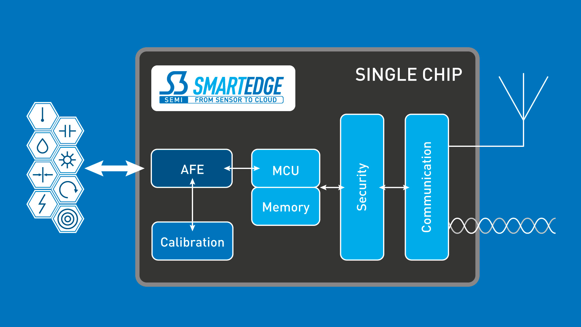
[Figure 1 | S3 Semiconductors – SmartEdge platform]
S3 Semiconductors, for example, have taken the custom SoC development a bit further by establishing a platform approach to designing an SoC for IoT/IioT edge applications. The ‘Smart Edge’ platform integrates the building block components together (Figure 1) in order to provide a highly optimized single-chip custom SoC. Accommodating different sensors is easily achieved with specific analog front end (AFE) IP blocks that are highly efficient at their given task ensuring that system designers can maximize performance for each sensor element (Figure 2).
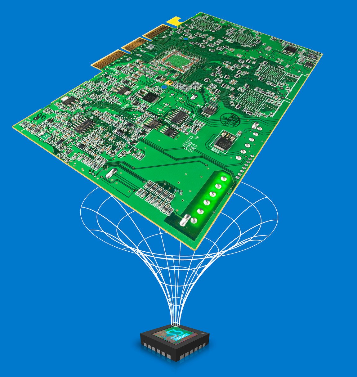
[Figure 2 | S3 Semiconductors – analog front end]
The result of this effort is an SoC that is optimized for the demands of the IoT node or system vendor at multiple levels – functionality, security, cost, and energy efficiency. The support of SoC implementation specialists who can advise on process, system architecture, circuit design, and software infrastructure considerations will ensure the project’s success.


