Excitation current mismatch effects in three-wire RTD measurement systems, Part 2
March 23, 2015

In Part 1 we introduced three-wire RTDs, lead resistance cancellation, and the benefits of designing a ratiometric three-wire RTD system. We showed th...
In Part 1 we introduced three-wire RTDs, lead resistance cancellation, and the benefits of designing a ratiometric three-wire RTD system. We showed that while a ratiometric RTD configuration removes the errors from the initial accuracy of the excitation currents, mismatch between the two excitation currents still causes a gain error.
In Part 2 we provide an analysis of an example integrated ratiometric three-wire RTD measurement system to understand sources of error, including the effects of the excitation current mismatch.
Integrated RTD measurement circuits
Typical integrated RTD measurement solutions include the excitation currents, gain stage, analog-to-digital converter (ADC), and other useful features such as open-sensor detection. These solutions greatly simplify the design compared to discrete systems while achieving high accuracy.
One example of a modern integrated solution with a 24-bit delta-sigma ADC that incorporates several features to facilitate the design of temperature measurement applications is the ADS1220. In this integrated solution, the excitation currents are controlled with current output digital-to-analog converters (DACs), also known as integrated DACs (IDACs). A multiplexer is included for easier routing of the IDACs to the resistance temperature detectors RTD circuit. Finally, a programmable gain amplifier (PGA) is used to increase the voltage resolution of the RTD system. A simplified circuit schematic using the integrated ADC solution is shown in Figure 1.
|
|

Sources of error in RTD measurement systems
The error sources in three-wire ratiometric RTD measurement circuits are the same whether the solution is integrated or built discretely. As shown in Part 1, errors from the magnitude of the excitation currents have been removed in the ratiometric measurement. However, errors due to the initial mismatch and temperature drift of the two excitation currents results in a gain error. Errors from the input gain stage, ADC, and tolerance of RREF also cause errors in the final measurement result. These errors appear as offset, gain, or linearity errors in the final measurement result.
Table 1 lists the ADC error sources that affect the RTD measurement.
|
|
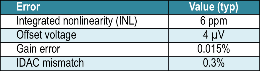
Since the input to the ADC is a voltage, integral nonlinearity (INL), gain error, and IDAC mismatch errors must be converted to an input-referred voltage as well. An example system is defined in Table 2 and Table 3. This system is used to calculate errors as an input-referred voltage. Selecting circuit values is outside the scope of these articles, but is described in detail in the TI’s reference design TIPD120.
|
|

|
|

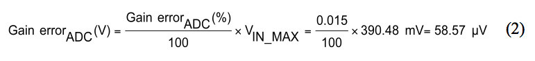
Using the example circuit configuration in Table 3, now the error sources can be referred to the input and compared against the maximum RTD voltage, which is 0.39048 V.
The PGA produces an input-referred offset voltage error that can be directly used in the total error calculation.

The gain error is specified as a percentage of the full-scale range, also known as %FSR. The input-referred voltage error can be calculated by multiplying the gain error by the maximum RTD input voltage, equation (2).
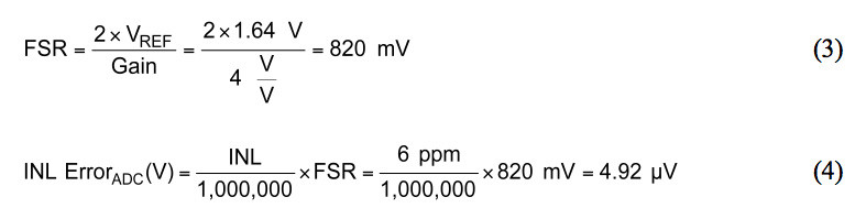
The INL is specified in parts-per-million (ppm) of the ADC full-scale range. INL is not a gain error. Therefore, it must be multiplied by the full-scale input voltage of the ADC rather than the maximum RTD voltage. The full-scale input in this configuration is given in equation (3), and the input-referred INL error is calculated in equation (4).
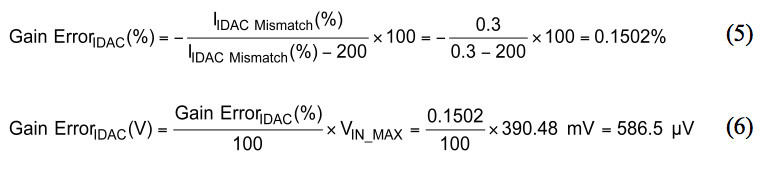
The IDAC mismatch is specified in %FSR. Therefore, the gain error and resulting input-referred voltage error can be calculated using equation (15) from Part 1. This is shown here in equations (5) and (6).
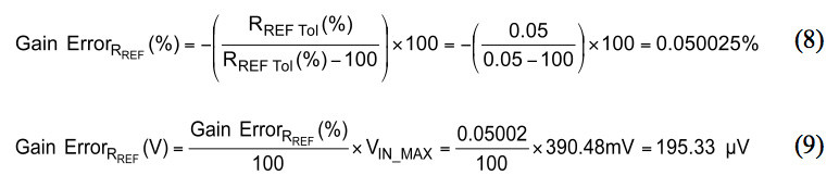
Errors from RREF tolerance
The last significant error source is the tolerance of RREF, which produces a gain error in the ADC transfer function. The gain error caused by RREF can be calculated using the same method used to calculate the IDAC mismatch gain error. The final result is shown in equation (7).

Assuming the RREF tolerance is specified as 0.05 percent, the gain error is calculated as shown in equation (8). The input referred error is calculated in equation (9).
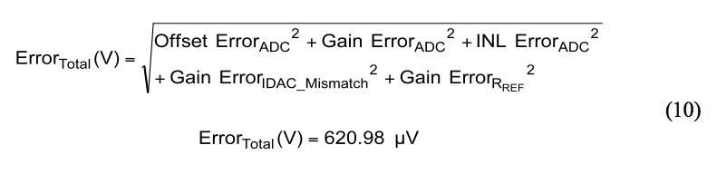
Total error at room temperature (TA = 25 °C)
Table 4 lists a summary of all errors for this ratiometric three-wire RTD system at 25 °C ambient temperature (TA). A probable maximum error can be calculated using the root sum of squares (RSS) of the input-referred error voltages. The IDAC mismatch accounts for roughly 95 percent of the probable total error.
Total error is calculated in equation (10).
|
|

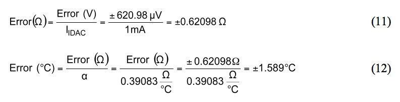
Equations (11) and (12) show how to convert the total voltage error in Table 4 to Ohms, and ultimately to degrees Celsius. The error in Ohms is converted to temperature using the sensitivity, α, of a Pt100 RTD as defined by IEC-60751.
Drift error (TA = -40 °C to 85 °C)
As mentioned in Part 1, standard room temperature calibration techniques can be used to remove the gain and offset errors from the system, leaving only the linearity error. However, unless an over-temperature calibration is performed, the temperature drift specifications still cause errors.
Table 5 displays the ADC temperature drift specifications. The temperature drift of the IDAC currents is the largest error source over temperature. The IDAC mismatch drift can be removed by techniques that we will introduce in Part 3. However, the offset and gain error drifts remain unless an over-temperature calibration is performed.
|
|
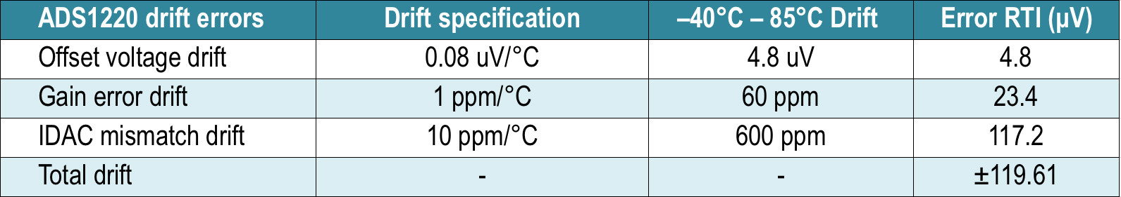
The total drift error accounts for an additional ±0.306 °C of temperature error over the -40 °C to 85 °C operating temperature of the system and is mainly due to the IDAC mismatch drift.
Summary
In Part 2, we analyzed the errors of an example ratiometric three-wire RTD measurement system based on the ADC’s specifications and external components. While a ratiometric system removes errors from the absolute value of the IDAC sources, any mismatch and mismatch drift between the IDACs results in an error. In many cases, as shown here, the IDAC mismatch is the largest error source. Also, the IDAC mismatch drift is the largest contributor to over-temperature errors.
In Part 3 we will discuss options to reduce or eliminate the errors caused by the IDAC mismatch and mismatch drift, leaving only the gain error, offset voltage, and INL errors from the ADC.
References
1. Download these datasheets: ADS1200, and ADS1247
2. TI reference design: TIPD120
3. Check out TI’s E2E community Precision Hub blog where you can search for related topics, including this one.