
Digital isolators can be used in intrinsic safety applications
May 03, 2018
Story

Designers of intrinsic safety equipment know the challenges of getting signals in and out of your equipment.
Designers of intrinsic safety (IS) equipment know the challenges of getting signals in and out of your equipment. New technologies are available that have tantalizing properties that would make a design smaller, simpler, lower power, faster, or all four, but it is not clear if or how you can use them because of the requirements of the IS safety standard.
If you are new to the world of intrinsic safety (IS), you might be a little overwhelmed by the terminology and concepts. It tends to be a world apart from the rest of electronic design and takes a while to come to terms with the terms and world view (pun intended). Let’s review the primary concepts behind IS isolator components. It is all about safety around flammable atmospheres and dust. The primary concept is that the design cannot be capable of creating a spark or flame with the energy available to it so that under every conceivable fault scenario, the insulation will remain intact. All of the testing and design guidelines laid out in IEC 60079-11 are really to achieve those two goals. The standard approaches the safety side by mandating insulation properties such as thickness or distance along the surface. While this is the common way to approach insulation safety, the safety margins chosen were much more conservative than is typical in IEC standards.
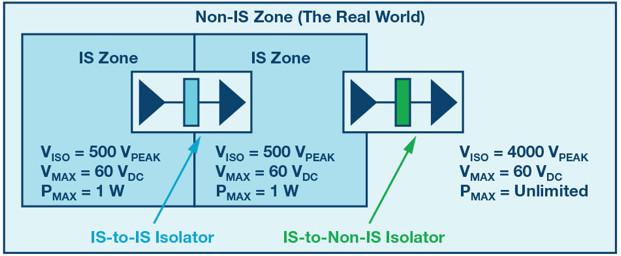
The world of intrinsic safety is divided into two zones: the intrinsically safe zone where dust and gas create hazardous conditions, and the rest of the world (the non-IS zone). Within the IS zone, energy is limited, and voltages tend to run in the 24 V to 60 V range with limited current and in the safety extra low voltage (SELV) range. In this environment, a component must be able to dissipate the maximum power that the system can provide it without sparking or burning. This can be achieved a couple of ways. One is to build rugged components that can dissipate a lot of power without heating up. The other is to protect the inputs and outputs with discrete components that will limit the power to what can be tolerated by the part. Typically, the limiting components consists of a Zener diode to limit the voltage and a fuse or resistor to limit the current. If you consider a modern system with even a modest number of components, this can start to become a large number of passive components surrounding every active component. The non-IS zone, where you and I live, has line voltages in the 100 V to 250 V range with potentially unlimited current. To be called safe, an isolating device must be able to survive a fault to the line power and not invalidate its insulation or cause an arc spark or burn that gets into the IS zone. That means very robust interfaces and protection devices capable of handling a very energetic fault. Robust protection uses even more and larger components and board space.
Did I mention that the IS standards committees are very conservative and do not adopt new technologies quickly? The technology of choice to get logic level communications between zones is the venerable optocoupler. There has been a strained relationship between optocoupler manufacturers and the conservative insulation requirements of the IS standard. The IS standard does not assume much about the quality of a piece of insulation, it only recognizes two types of insulation. The first is a casting compound that can cover relatively reliable mold compounds for ICs, as well as potting compounds that are far less controlled. The second type of insulation is everything else that is solid and insulates, which would encompass everything from glass and thin polymer films to wax paper. The capabilities of these insulation materials and the quality of their application may vary widely. The standard takes the conservative approach and mandates thick layers of insulation. When an optocoupler was designed with the minimum thickness prescribed in the standard, it became difficult to make a component that functioned with any kind of speed. Efforts were made over the evolution of the standard to reduce the through-the-insulation requirements, allowing better performing optocouplers to be used. New testing was created, the optocoupler carbonization test, to verify that optocouplers would not rupture when the very high power available in the non-IS zone was applied. The results were mixed at best and most designers and optocoupler companies were not satisfied with the compromises.
[Figure 1 | Isolation layout of an intrinsically safe system.]
Requirements of IEC60079-11
The IEC60079-11 standard, explosive atmospheres section—Part 11: Equipment Protection by Intrinsic Safety “I” Edition 6—contains the guidelines for making a system safe for use in explosive environments such as chemical plants or areas with combustible dust. The standard characterizes isolator devices in four ways.
Distance around the insulation and along the surface, creepage, and clearance
Creepage and clearance of the package depend on the required working voltage and installation class, based on IEC60664 insulation coordination and pollution degree 2 or 3, depending on the application.
Fault tolerance
Faults to the highest available system voltage must be tolerated without burning, arcing, or invalidating the insulation. This may require external components or not depending on the available energy. This is about insulation integrity in high temperature environments—it does not require component functionality.
Transient rating
This will be derived from the installation class and system voltage for SELV type environments. Inside the IS boundary, this will commonly be 500 V rms, and for line voltages it may be as high as 6000 VPEAK. This characterization is about insulation integrity to high voltage stress. It does not require component functionality.
Distance through the insulation
The insulation coordination standards simply state that insulation punch through and wear out cannot be reliably predicted and must be derived experimentally. In the case of IS-non-IS barriers, the IEC60079-11 standard chose to err on the side of safety and chose values for distance through the insulation large enough that almost any insulation would be safe. For line voltages, this means 1 mm to 2 mm of insulation are required, and for controlled environments, 0.2 mm is required. In the case of IS-to-IS interfaces, the distance through-the-insulation requirements are not applied.
There are two barriers that must be traversed in an IS application, the IS-to-non-IS barrier, where line voltage is present on the non-IS side, and the IS-to-IS barriers internal to the intrinsic safe zone, used to segregate energy within the system from distributed capacitance or power supplies. The power is usually at SELV levels. The standard puts very different requirements on isolators at each type of barrier.
Isolator properties
How do the IEC60079-11 requirements affect the designers ability to use an isolator in an IS application? The creepage and clearance distances required and transient ratings are similar to what is required by any industrial standard. Nearly all optocouplers and digital isolators can comply with these requirements. What determines the suitability of an isolator are its ability to tolerate a fault condition and the through-the-insulation distance required in Table 5 or Annex F of the IEC60079-11 standards.
Optocouplers have been around for about 50 years. They are the standard technology that has been available to IS designs to get logic-level signals in and out of an IS zone. It was realized early on that the insulation and power dissipation requirements were onerous for optocouplers. For example, a 1 mm through insulation requirement attenuates the light so much that high speed optocouplers are not practical. Low speed optocouplers can be made, but their performance is compromised.
The standard was changed over the years as the industry required more and faster communications. Two efforts were made to accommodate optocouplers. The first was Annex F, which was formulated for a cleaner installation environment (pollution degree 2) than was assumed for the body of the standard. This allowed creepage and clearance to be shorter. In addition, the through-the-insulation distances were lowered to 0.2 mm, which allows most optocouplers to meet the requirement. Second, a special test section was added to characterize optocouplers for faults in the IS-to-non-IS boundary without the need for external limiting components. This section includes a lot of overload tests and something called the carbonization test. Unfortunately, this set of tests was so severe that few optocouplers were ever qualified to this portion of the standard.
The standard had now accommodated optocouplers enough that workable interfaces can be made using them. However, the same shortcomings that optocouplers have in all industrial applications are an issue in IS applications. Namely, optocouplers are now large, slow, power hungry, limited in their ability to integrate other functions or even channels in mixed directions, and their parameters drift over time.
The alternative technology is the digital Isolator, which can address almost all of the functional issues of the optocoupler. Digital isolators can operate with ultra low power, very small packages, multiple channel directions in a package, speeds an order of magnitude higher, easy integration of interface functionality, and stable performance over time. These properties make them very attractive to the designers of IS equipment. However, in order to achieve these features, they use thin film insulation that can be in the 10 μm to 40 μm thickness range. Referring back to the through-the-insulation requirements of about 1 mm for Table 5 or 0.2 mm for Annex F, the digital isolator has insulation that is much thinner than those requirements. At this point, most designers heave a heavy sigh and start flipping through the optocoupler catalog again.
Not so fast! As you will recall, the distance around the insulation and along the surface, creepage, and clearance does not apply to IS or to IS isolation, so the digital isolators can be used in that boundary. In the IS-to-IS applications, the voltages are usually limited to below the SELV voltage limits and power is limited as well so transient isolation is usually 500 VPEAK and the creepage and clearance are only 0.5 mm to 4 mm depending on the table used. This means that in these interfaces, the small packaging offered by the digital isolator can be utilized. Suddenly the digital isolator becomes very attractive. The only matter left to address is the fault tolerance.
In the limited voltage and current environment of the IS-to-IS boundary, fault tolerance can be dealt with in a couple of ways, by protecting the I/O pins and power supplies or by designing and qualifying the pins to dissipate sufficient power. The external protection option consumes a lot of board space and may take more space than was gained by going to small packaging. The other option is to evaluate the device for its behavior under fault conditions from which entity parameters are generated. Entity parameters are a set of limits for voltage, current, and power that will guarantee that the part will not arc, rupture, or invalidate its insulation. Under these conditions, the part will likely experience a temperature rise from the dissipated power. This, combined with the maximum rated ambient temperature, will give a maximum package temperature that is used in the IS thermal analysis.
Practical example: Analog Devices ADuM144x Quad Isolator
Analog Devices’ ADuM144x series of iCoupler digital isolators is of interest to IS system designers for several of its properties. It can consume power in the microampere range, has a high data rate of 2 Mbps, and has 4 data channels in a small QSOP or SSOP package with insulation capable of withstand. The creepage, clearance, and transient specifications (in excess of 6000 VPEAK) of these digital isolators are more than adequate for the IS environment. The device is well suited for 1 Mbps SPI communications. The part specifications make the part attractive to IS applications, as having an evaluation to IEC60079-11 make it easily usable.
This family of devices, as with all digital isolators, does not have thick enough insulation for an IS to non-IS isolation and it had not been evaluated for entity parameters. This means that the device could be used with external protection devices in IS-to-IS barriers. However, the part was capable of tolerating a fault to high enough power dissipation that, with the proper testing entity parameters, could be generated that would allow the device to be used without protections—making it ideal for the IS-to-IS environment.
Analog Devices worked with CSA/SIRA to generate ATEX and IECEx certifications for this family of devices to allow IS system designers to easily include it in their designs. CSA/SIRA had to interpret the requirements of the existing standard as they apply to digital isolators. For example, the pulse transformers used in these devices are closer to capacitors as far as their insulation properties. They store very little energy, so it did not make sense to apply the transformer design rules to them. The procedures for testing for entity parameters had to be developed from scratch as well.
The entity parameters and environmental conditions are shown in Table 1 and Table 2. The power dissipation is specified to maintain insulation integrity, not part functionality past the safety aspects. This allows higher power dissipation to be specified and external components to be eliminated. It should be noted that all entity parameter limits must be met in order to guarantee insulation safety so the total power will limit either voltage and/or current in practical application. The maximum surface temperature in Table 2 reflects the measured max surface temperature seen in characterization. The larger package has the lower temperature. This is the first digital isolator to carry a general component level certification for use in explosive environments, and it therefore meets all of the manufacturing quality requirements of the standard.
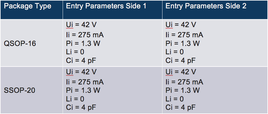
[Table 1 | ADuM144x Entity Parameters]
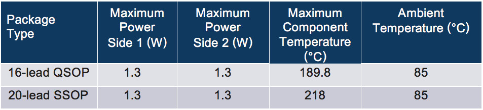
[Table 2 | ADuM144x Thermal Characteristics]
What does the future hold?
Having a limited use digital isolator is great in some circumstances, but the application of overly conservative nonspecific insulation thickness requirements to all types of isolators has given rise to either restricted usage or performance restricting construction. The IS community has long recognized this and the issue is being addressed at the standard level. A new approach to IS isolators is being examined for inclusion in the next revision of the standard that would treat both optoisolators and digital isolators uniformly and provide an alternative to the through-the-insulation requirements in the current version of the standard. The fault tolerance testing required to avoid use of external protection devices is also being streamlined. The future will hold much more access to high performance digital isolator devices in intrinsic safe applications.


