
Bit-by-bit towards an industrial storage solution
November 13, 2017

Developers need to understand the basic mechanisms of storage and effects at the storage level to know which flash memory products are most suitable for a particular applications.
Triple-level cell (TLC), multi-level cell (MLC), single-level cell (SLC), pseudo single-level cell (pSLC) – there are many flash memory technologies. Developers need to understand the basic mechanisms of storage and effects at the storage level to know which flash memory products are most suitable for a particular applications. Only then will they know what questions to ask suppliers.
Different aspects of an application can determine the selection of a memory module for embedded industrial systems. These include read and write speed, endurance (or the lifetime of flash media), retention (the lifetime of the stored data), data security in case of power failure, temperature and vibration resistance, long-term availability of a product, and more. The aging of NAND chips, a flash-specific effect, plays a significant role in the decision-making process as well.
The cells of a NAND flash device only survive a limited number of block erase cycles. In the oxide layer, which separates the storage gate, electrons with increased energy levels (hot electrons) become trapped after being accelerated by the programming voltage. In due course, this shifts the threshold voltage until the cell is no longer readable (Figure 1).
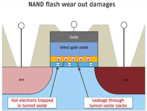
Figure 1. An aging cell: Electrons gather in the tunnel oxide layer, which gradually shifts the threshold voltage value. Cracks in the tunnel oxide create leakage current paths, which allow the charge to leak off. The read errors increase until the complete block has been rejected as a “bad block”.
Flash aging – When does it end?
There is also a second aging effect: The formation of conductive paths through the oxide layer. This causes the cell to gradually lose its charge state, and thus the stored bit.
High temperatures amplify this effect considerably. Studies using a 25 nm MLC NAND device have shown that after five years at 55 °C, retention drops to approximately 75 percent. At 85 °C – a comparatively moderate increase – retention drops below 10 percent.
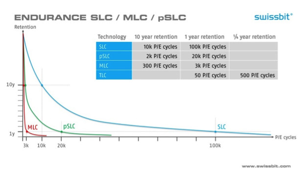
Additionally, the effect becomes stronger over time, as a cell gets closer to its maximum program erase cycles (P/E cycles). The impact on retention here is massive. For example, a low-cost MLC NAND flash device's original retention capacity of 10 years can drop to roughly one year after reaching 3,000 P/E cycles.
Similarly, the charge state and threshold voltage challenges of lower-cost TLC NAND flash chips require eight different distinguishable charge levels in order to write three bits per cell. The degenerative effects are noticeable much more quickly in these designs, with original retention timetables degrading from one year to three months after only 500 P/E cycles.
While more costly SLC devices experience the same degradation, approximately 100,000 P/E cycles must occur before these effects take place. The significantly higher P/E cycle tolerance is an important reason why, despite their higher cost, SLCs remain the preferred flash technology for industrial applications.
The cost compromise: pSLC
The pSLC process was introduced to balance cost with the realization that a reduction in the number of different charge levels make data storage on a NAND chip more robust. Compared to SLC, pSLC uses a more cost-effective MLC chip for the first "strong" bit per cell, with some astonishing results. The pSLC mode is significantly faster than standard processes on MLC flash memories, and increases the number of P/E cycles before degradation from 3,000 to 20,000. Under the same conditions, data endurance is improved 6.7x at only twice the cost per bit stored (Figure 2)
Caution with endurance specifications: The workload is decisive
Developers need to know exactly what a manufacturer's specifications represent when selecting a storage device. Two measurements in particular indicate the endurance of an SSD: Terabyte written (TBW) and drive writes per day (DWPD). TBW indicates how much data can be written in total during a device's lifetime, while DWPD indicates the maximum amount of data that can be written per day during the warranty period.
The challenge with sometimes-elaborate manufacturer specifications is that developers can't be certain whether they have any significance to the application in question. Specification values depend heavily on the type of workload during test. For example, a 480 GB SSD from Swissbit exhibited endurances of 1,360 TBW, 912 TBW, and 140 TBW depending on measuring procedure. Sequential writing produced the strongest value of 1,360 TBW, while "client workloads" and "enterprise workloads" accounted for the second and third values, respectively. The client workload was based on the behavior of a PC user generating mainly sequential data access operations, while the enterprise workload simulated the behavior of a multi-user server environment in which 80 percent of data was accessed randomly.
Such endurance tests are based on guidelines set by the JEDEC standardization organization, and help ensure the comparability of products and manufacturers. More often than not, however, workload specifications are not included in datasheets. Many manufacturers happily advertise phenomenal endurance values based on sequential writing used in only a few applications. As illustrated in the above example, endurance values of a flash solution can easily differ by factor 10 for sequential writing and enterprise workload. Buyers must exercise caution.
Stressed flash memory
The aging of memory cells is accelerated by erasure; however, block erasures are required in order to write. This could lead to the deceptive conclusion that in a pure reading application, like a boot medium, data is secure in the long-term due to its extended retention. Unfortunately, this is a misconception. There are other circumstances that cause read errors and indirectly cause wear and tear of NAND cells.
During each writing process, cells adjacent to the cell being programmed are stressed. These show a slightly increased voltage, referred to as "program disturb." Reading causes stress as well "read disturb," where the neighboring pages collect voltage. Over time the stored potential in these cells increases. This causes read errors, which, after deletion of the block, disappear again. Due to the lower voltage, the effect is weaker for reading than for writing, but bit errors occur nevertheless. These are compensated for in error correction code (ECC) by deleting the block.
However, developers still have to consider that the effect is particularly strong in applications that repeatedly read the same data, meaning that even inside a memory medium that is only used for reading, blocks have to be deleted and pages written regularly as part of the error correction. As a result, this medium ages as well.
Internal concerns
This medium aging leads to “internal concerns” of a flash memory device. Erasure, writing, and reading are not only triggered by the actual application, but also by numerous controller and firmware processes. What happens here often goes unnoticed, but can again influence performance factors such as speed and endurance.
In addition to error correction, another of these internal mechanisms is wear leveling. When a cell fails, the complete block has to be marked as a “bad block.” For endurance purposes it is important to delay this failure if possible. This can be achieved using wear leveling, which is an even distribution in the use of physical memory addresses. Another internal mechanism is garbage collection, a re-copying for the release of blocks.
These processes complement the mechanism that makes data storage possible in the first place: mapping between the logical and physical address. The efficiency of the controller of a flash medium is measured by the ratio between the user data coming from the host and the actual data value written onto the flash memory. This is expressed using the write amplification factor (WAF).
Reducing the WAF is one of the keys of longer endurance. There are workload factors that influence the WAF, such as the difference between sequential and random access, the size of the data blocks in relation to a page, and the block sizes themselves. As a consequence, the firmware also determines whether a flash medium is suitable for an application.
How manufacturers increase efficiency
For a better understanding, another discourse about the operating principle of flash memories follows. The pages of a block of cells have to be programmed in succession, but only complete blocks can be deleted. Mapping between the logical and physical address refers, in the standard process, to blocks. This is very efficient for sequential data because the pages of a block are written in succession. Continuously collected video data is one example of an application for which the block-based allocation is ideal.
This is different for random data. Here, pages are written in many different blocks. This means for each internal re-programming, a complete block has to be deleted per page. Consequently, the WAF is high and endurance decreases. Thus, page-based mapping is better suited for non-sequential data. Here, the firmware ensures that data of different origins is saved sequentially on the pages of one block. This reduces the number of deletions – with positive effects for endurance – and the write performance increases. However, page-based mapping increases the allocation table of the flash translation layer (FTL). Manufacturers compensate for this with integrated DRAM. Therefore, the benefits of page-based mapping are not fruitless.
Abundant over-provisioning as quality feature
Page-based mapping is also beneficial if the degree of utilization of the data medium forces the WAF up. The more data is stored on the flash medium, the more bits have to be moved back and forth by the firmware. Manufacturers are able to prevent problems with overloaded data media by simply over-provisioning. This refers to the flash area reserved for only internal activities. Conventionally, this is 7 percent of the total area that, with gigabyte specifications, make the difference between a decimal and binary value.
If 12 percent rather than 7 is reserved for over-provisioning, a surprising effect is created. For an endurance comparison (TBW for enterprise workload) of two SSDs with identical hardware, the 240 GB Swissbit model X-60 durabit with 12 percent of its area reserved for over-provisionng achieved a value almost twice as high as a model with 256 GB. If one then looks at the impact of the DRAM on endurance, the difference for the 240 GB durabit version is 10 times higher compared to the standard version with 256 GB (Note: As already achieved when using MLC as pSLC, a significantly positive endurance effect can be reached by foregoing memory capacity or by applying over-provisioning).
Data maintenance
Error correction and wear leveling are mechanisms that are also used in universal flash products. For high-quality industrial SDDs or flash memory cards, the manufacturers take further efforts to prevent data loss and system failures. Thus, the combination of different mechanisms such as ECC monitoring, read disturb management, and auto read refresh ensures that all stored data is monitored and refreshed as required. This allows the prevention of system failures in advance. (Note: Data integrity should be ensured without involving the host application. This allows processes to run autonomously within the memory card – not just when cumulative bit errors follow read requests by the host application, as is usually the case).
Thus, advanced data care management searches independently of requests by applications for potential errors (Figure 3). For this, all written pages, including the firmware and the allocation table of the FTL, are read in the background and refreshed as required. There are various triggers for this preventative error correction, including a defined number of repeated switching on the number of P/E cycles, the read data volume, read repetitions/re-readings, and also increased temperature.
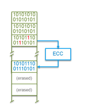
Figure 3. Data care management counteracts gradual data loss. Thus, all written blocks are read in the background and, in case too many bit errors are copied, repaired and rewritten.
Knowing what to select
Knowing the different aspects of flash technology is the key to selecting the most suitable storage solution for industrial applications. Naturally, criteria such as power-fail protection mechanisms, particularly robust processing, and the specification for an extended temperature range should be considered as well.
Long-term availability of modules that were specified for a particular application is important as well. This is why one type of flash memory – 3D NAND – has not been represented here at all. This technology is still too new to ensure long-term availability, and innovation cycles and design changes are still too ad-hoc for industrial product lifecycles.
Ultimately, empirical values for the endurance and data retention of these NAND flash devices is critical during the selection of industrial storage technology. Optimization of these values is a key task for manufacturers of industrial flash products, and customers should press them on these numbers before they buy.
Key questions to ask:
- Do I have particular physical requirements regarding vibration resistance and the temperature range of the medium?
Industrial flash memories should have high-quality tested material properties and good processing, that can be proven by relevant qualification.
- Is the memory going to be exposed to high temperatures over longer time periods?
As high temperatures weaken the readability of cells faster, it is best to choose a product with data care functions that regularly refresh data.
- Is a lot of data to be stored on the data medium over a long period and maintained for a long time?
An SLC product is best suited.
- Does my application mainly read?
A medium with data care management that refreshes data regularly is recommended.
- Does my application mainly write?
A product with block-based mapping is suitable for sequential writing; for random access, a product with page-based mapping should be selected.
- Will the capacity of the memory be fully used?
With intensive use, the controller needs space for internal processes – over-provisioning extends endurance.
- Which workload has the manufacturer based his TBW and DWPD specifications on?
Data media can only be compared using the workload benchmark.
- Do I need increased data loss protection?
For particular critical applications, data care management and power fail protection should be included.
- Will the medium still be available in a few years' time?
The manufacturer should warranty long-term availability to allow replacing the memory without the need for re-qualification.
Ulrich Brandt is Director of Marketing at Swissbit AG.
Swissbit


