
X-FAB Launches High-Voltage Galvanic Isolation Process Technology
January 30, 2019
Product
This plays an important role in controlling industrial/automotive IGBT or SiC power modules, as well as in field bus data communication systems, battery management systems, and medical equipment.
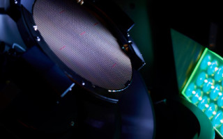
X-FAB Silicon Foundries announced the full-volume production release of its new high-temperature galvanic isolation semiconductor process. This proprietary technology is fully automotive qualified and offers high levels of reliability.
Key advantages of the new X-FAB galvanic isolation process include:
• Operational temperatures of up to 175°C
• Successfully tested up to 6,000 Vrms @ 50 Hz and 10,000 VDC
• Uninterrupted barrier layer with 0 ppm residual contamination
• Demonstrated conformance with latest IEC 60747-17 semiconductor coupler draft standard
• Support for working voltages up to 1.7 kV
X-FAB offers two types of packaged galvanic isolation devices for customer evaluation. The capacitive coupler test chip, G3-C1, has an isolation layer thickness of 11 µm and was tested to withstand up to 6,000 Vrms (the maximum limit of the test setup). An inductive coupler test chip, G3-T06, is also available for customer evaluation and has an isolation layer thickness of 14 µm.
Design kits for all major EDA platforms can be downloaded from X-FAB’s customer web portal. Samples and full process qualification reports are available on request.
For more information visit www.xfab.com.


