
Mind the gap: Going from reference board prototype to production system
January 20, 2018
Blog

Embedded systems designers need to look beyond prototypes at how they will be transformed into products. The path from prototype to a production-worthy design is not as simple as one might expect.
Once you have your idea for an amazing, innovative product, building a quick prototype is not the challenge. The challenge is creating a high yield, high quality, and highly valued design.
The market is filled with evaluation and development boards that have capabilities such as wireless communications, high-performance processors, high-speed memory, power management systems, and complex analog peripherals. Additionally, there are many open source communities and tons of available reference code that allow design engineers to minimize development time while optimizing the features of their product.
However, an embedded systems designer needs to look beyond just the prototype at how it will be transformed into a sellable product. The path from prototype to a production-worthy design is not as simple as one might expect. Early decisions about components can save significant opportunity cost when designing and manufacturing a commercial product down the line.
Product after prototype: Keeping an eye on the prize
Once a prototype is complete, the challenge for the embedded design engineer becomes how to quickly convert the prototype into a commercial product. This requires generating a set of schematics and layout that can be manufactured within the product’s size and mechanical design constraints.
The quick answer is to turn to a development board’s specs online and get started with it as the basis for the product design, right?
Unfortunately, when using a development board as a reference design, embedded designers may not be aware of some of the pitfalls associated with replicating that design in a commercial product. First, not all development boards have open schematics and layout. Second, it may be difficult for smaller companies to procure parts for their production designs since they might not meet minimum volume requirements. Even if parts are procurable and the reference files are freely available, errors and inefficiencies in development board designs often carry over into production systems. Add to this the time and engineering skill required to work with complex layouts, and a significant amount of talent can be squandered on issues that add little value to an end product.
For example, most connected embedded systems need the software capabilities provided by Linux, which require powerful processors, high-speed memory, and sophisticated power management. Plenty of development boards have these features, but this integration may have to be laid out from scratch when designing a production system. Laying out a PCB for the DDR memory and processor alone requires matching 30 to 40 DDR signals to ensure that timing and impedance specifications are met. This is a tedious and often time-consuming task, but just having a working DDR interface doesn’t differentiate a product.
Think of the aforementioned processor and memory interface task like good electrical wiring in a house – you need it, and you would not be able to sell a house without it, but it adds no value to the price of your home. Similarly, spending the time to become an expert in some routing tasks does not add value to an end product. Instead, designers need to be spending time adding unique value rather than redoing complex routing tasks.
Beyond the traditional schematic and layout expenses, the cost of manufacturing these complex boards can also increase exponentially if care is not taken during the initial product design. For instance, sourcing components that don’t fit within traditional pick-and-place or reflow manufacturing processes can be pricey.
With all of these factors in mind, embedded design engineers evaluating a development boards should consider:
1. What the development board is not:
- What are the dimensions and shape of your final product?
- What set of components will your product use?
- What is the optimal number of PCB layers for your product?
- What is the best set of design rules for your product?
2. What the production design needs to be:
- The right form factor (form, fit and function)
- The right set of components (in terms of specification, availability, and cost)
- Producible in your volumes with high yields and minimal cost
- Testable and repairable
Integrating value in commercial products
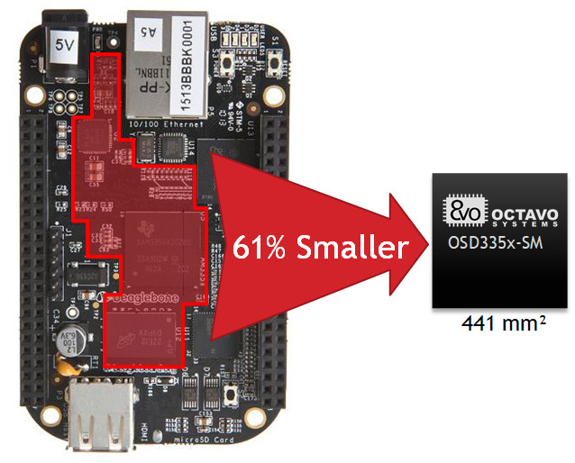
One solution to some of the problems highlighted has been around for a while: system on modules (SoMs). SoMs mimic the core functionality of a development board by integrating some of its components into a single module, which simplifies many design challenges up front. However, manufacturability with SoMs can be non-standard adding special handling and costs.
Fortunately, there is a better bridge between reference boards and production: system-in-package (SiP) devices. SiPs combine a number of integrated circuits (ICs) in one highly compact module that function as a single integrated unit. They utilize advanced IC packaging technology to create building blocks for design engineers, which can include components such as high-end DDR memory, multicore processors, power management systems, discrete logic, sensors, and hundreds of passives. Any number of devices from any silicon process can be incorporated into a small, complete, ready-to-use subsystem. Instead of building with raw plastic chips, design engineers can now use Legos.
SiP technology was born out of the overwhelming success of Moore’s Law, which has allowed semiconductors to be produced that are less expensive, higher performance, and dissipate less power. Simultaneously, however, Moore’s Law has also created a world in which no one semiconductor manufacturing process works best for all types of components. For example, high-performance, high-density silicon processes work well for microprocessors and memory, but is not as effective for sensitive analog components or MEMS devices. This is one of the drawbacks of system on chips (SoCs), as they must compromise on a single silicon process.
SiPs: A new era of ICs
Beyond being able to integrate ICs and passive components from different silicon processes that would be impossible to create on a single wafer, SiP devices offer many tangible benefits when moving from a prototype to a production design.
First and foremost, SiP devices remove complex, mundane, non-value-add design tasks. Similar to SoMs, SiPs integrate components at the heart of a system such as the processor, high-speed memory, and power management. But SiP technology takes this integration to the next level as devices that have the same look and feel as a standard IC, just with better signal integrity, lower power consumption, and a smaller, connector-less form factor than you get with a bulky module. By removing complex routing and power management from the system design, SiP devices also reduce the number of PCB layers required in a given design.
Another benefit of SiPs is manufacturability. Given that a SiP device looks like a standard packaged IC, it fits well within low-cost pick and place or reflow manufacturing processes. As mentioned, SiPs can integrate hundreds of discrete components, which reduces manufacturing time and the cost of products. In addition, the ability to integrate passives enables single-sided designs for complex microprocessors that would otherwise have to be placed directly under the device.
Finally, SiPs simplify the supply chain. Sourcing components in small quantities at a reasonable cost can be a real headache as a design moves to production, while trying to guarantee availability hundreds of components at the time of manufacture can be a daunting task. Using a SiP, sourcing is already done. Instead of worrying about the lead time of a hundred components, you now only have to worry about the lead time of one. Although this might not be a huge advantage for design engineers, operations people will thank you.
Make the most of Moore’s Law when moving from prototype to production
While the performance, features, cost, and community support of a development board can be attractive, choosing the right devices for your end solution first will ease your path to a successful product. The best of the best processor, memory, analog, and power technology for a given design can be leveraged in integrated packages that take full advantage of Moore’s Law, so why compromise?
So, the next time you are looking for a development board, ask yourself, “Does it have a SiP?”
Erik Welsh is Applications and Systems Manager at Octavo Systems.
Gene Frantz is Co-Founder and Chief Technology Officer at Octavo Systems.
Octavo Systems
LinkedIn: www.linkedin.com/company/octavo-systems-llc
Facebook: www.facebook.com/octavosystems


