
Embedded memory systems 101
April 25, 2016
Story
Memory subsystems needn't require a significant learning curve. The complexity of today's embedded systems and the accompanying memory subsystems can...
Memory subsystems needn’t require a significant learning curve.
The complexity of today’s embedded systems and the accompanying memory subsystems can sometimes have a learning curve for the novice engineer. Memory comprises hardware components that operate as either temporary (volatile) or persistent (non-volatile) storage “containers.” These magical nuggets of electrically-charged circuitry store states of information and are used for instructions (binary code) and organize data as addressable bytes (8 bits), double-bytes (16 bits), and quad-bytes (32 bits).
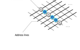
In combination with the embedded operating system (OS) that controls the resources like memory subsystems, software instructs the processor (CPU) to send a burst of electricity along an address line that identifies a transition’s location in the chip where data is stored. This pulse can turn on or off a transistor connected to data lines. When the electrical pulse reaches an address line, the pulse flows through a closed transistor and charges a capacitor that stores the equivalent of a 1 (on) bit and, conversely, an uncharged capacitor represents a 0 (off) bit.

1. Array of memory bits of information (partially shown).
Volatile memory is used as random access memory (RAM). Its contents are maintained only when power is applied. To complement RAM use, it was common in early embedded systems that read-only memory (ROM) was used to run the operating system and applications. Either memory source could be accessed in byte (8-bit) units of information.
Non-volatile memory retains data. For traditional PCs, Macs, and servers, persistent memory storage has been used to store a larger addressable container of bytes—usually organized based on an underlying grouping (known as a sector). Physical size and low power requirements have typically not been a priority for storage systems like fixed-disk or solid-state devices (SSDs). Not so for small embedded systems where size and low power are critical. This persistent storage media is either removable (SD or CF card, or USB flash drive) or non-removable, and its contents should be maintained regardless of the presence of a power source. Blocks of 512 and 4192 kbytes are popular sizes for these small devices. Given the small form factor of many embedded systems, device memory requirements and physical space constraints often dictate the types of memory that can be used.
Volatile memory basics
Volatile memory can be used for reading instructions executed by the CPU resulting in some operations being performed with data sometimes written back to memory. Today’s powerful embedded CPUs can process and access information as 32-bit (or even 64-bit) values. The days of 8-bit computing are long gone.
RAM is organized in one or more chips and can reside within the same package substrate along with the CPU and I/O ports, known as a system-on-chip (SoC), which is common in small devices (like drones, home sensors, etc.) where available board real estate is limited.
Non-volatile memory basics
Originally called flash RAM, flash memory is becoming the preferred permanent storage media, supplanting the rotating disk. Dr. Fujio Masuoka invented flash memory in 1984, while working at Toshiba. His colleague, Mr. Shoji Ariizumi, came up with the name flash because the process of erasing data from the cells reminded him of a camera flash.
Flash memory is a form of non-volatile memory that’s electrically programmed for long-term storage. The original electrically erasable programmable read-only memory (EEPROM) devices consisted of a grid of columns and rows with transistors at each intersection. A thin layer of oxide separated each transistor from the others. If one transistor (the floating gate) is linked with another (the control gate), the cell has a value of 1. If this link is broken, the value becomes 0. To change the value of a cell set to 0, a process called Fowler-Nordheim tunneling takes place, which changes the cell’s charge level. When power is removed, the cell is expected to retain its last setting (as programmed or erased).
The perception that flash memory is only for consumer mobile devices, like cameras and smart phones, is not true. In any system where the form factor is constrained and permanent data storage is required, flash memory is frequently used. Flash memory is either resident (soldered onto the board) or non-resident (removable devices through an industry-standard port like SD and USB). The beauty of flash memory is that there are no moving parts that could negatively impact reliability, but like any technology, there are pluses and minuses, as shown in the table.
| The Good | The Not So Good (Bad) |
|---|---|
| The size of the part (package) can be quite small – the latest generation of high-capacity USB flash drives are barely larger than the connector itself. | Flash is actually susceptible to wear, especially as flash memory gets smaller and smaller. |
| Low power consumption. | As flash technology improves, part obsolescence impacts OEM production cycles. |
| With no moving parts (like rotating media), device reliability can be great. With no physical disk head movement, heat is not an issue, random I/O performance should be quite good. | Differences in chip fabrication processes can impact quality, timing, and performance even from the same flash manufacturer with the same part number. |
| Individual flash memory cells are susceptible to bit disturbance and require sophisticated error detection and correction (EDC) algorithms. | |
| Loss of power at the wrong time and without proper protection can result in incomplete writes or erases. | |
| Where deleted data must be wiped leaving no trace, flash memory’s ability to assure a complete erasure is in its infancy. |
The good and the bad of flash memory.
There are two basic types of flash memory commercially available—NOR and NAND. NOR was originally designed to replace ROM, EPROM, and EEPROM non-volatile memory. It has a full set of address lines which allows reads of individual bytes. In fact, reads are typically as fast as DRAM, allowing programs to be run XIP (eXecute In Place), directly from NOR memory. Erases, however, are very slow and not a problem as long as erase operations are performed infrequently. NOR was originally used in removable compact flash (CF) cards, and was a good choice for storing OS images, system boot loaders, and system configuration information.
NAND was developed to achieve higher capacities, smaller footprints, and lower cost when compared to NOR. However, it’s restricted to a serial interface. Hence, individual bytes can’t be directly accessed; reads, writes, and erases must be performed in chunks (or blocks). This technology is an unsuitable replacement for ROM, but fits nicely as a replacement for hard-disk drives. NAND has become the standard flash technology for both removable and resident media, and, as a result, it’s suited for applications requiring low-cost, high-density, and fast erases.
Note the difference between blocks and pages. Each block consists of a number of pages where a page size typically is either small block (512 bytes) or large block (2048, 4096 bytes, and so on). The block size is important because you’ll typically get the best results if record sizes are an even fraction of the underlying block size used on the flash media. For all NAND, data is written as pages, but a page must have already been erased (to all 1s) and only blocks can be erased.

2. Pages and blocks.
No discussion about NAND would be complete if we didn’t mention how memory cells are organized to store bits of information. A single-level cell (SLC) stores one bit of information per cell. As storage capacity has increased, multi-level cell (MLC) and triple-level cell (TLC) have been developed to store multiple bits per cell. But this increased capacity has some disadvantages. MLC’s write performance is typically about one-third to one-half as fast as SLC. Its increased complexity also creates more bit errors, requiring more sophisticated error- correcting codes (ECCs) to prevent common data error conditions. TLC has even slower transfer speeds, higher error rates requiring even greater ECCs, and lower endurance than its SLC and MLC counterparts. Endurance is better when blocks are written a minimal number of times.
Typical NAND requires a controller to handle commands and data movement between the host computer and the flash. The controller provides the mechanism to perform basic operations like block reads, writes, and erases. Many designs include a discrete controller that provides only these functions and leaves other flash-management activities, like replacing blocks that go bad and ensuring even wear, to driver software. Some chip designers have found that efficiencies can be gained by including a built-in controller with the NAND flash in the same physical package called managed NAND. These sophisticated controllers offload some of the more compute-intensive software management at the expensive of higher chip cost, as shown in Figure 3.
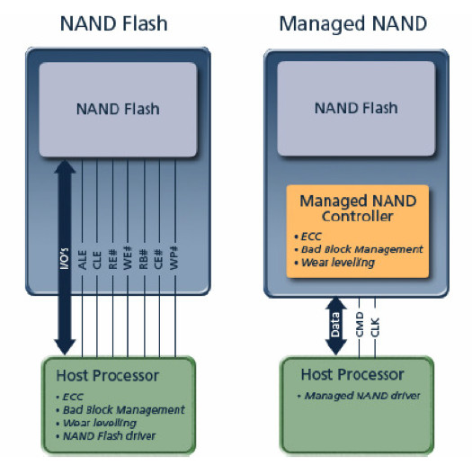
3. NAND flash versus managed NAND
This effectively enables the part to behave like a typical block device with a simpler interface for the host file system. As the price of managed NAND rivals the price of NAND itself, it’s no wonder that embedded boards incorporate resident managed NAND as an embedded multimedia memory card (eMMC) instead of flash and a controller.
Though it represents a great leap forward in taming the idiosyncrasies of NAND, eMMC is not a perfect technology. After running a series of performance benchmarks on eMMC 4.3 parts, Datalight’s engineering team observed lackluster performance on some parts, particularly with random reads. With one specific eMMC part, random I/O performed on files larger than 16 Mbytes slows down to a 200-byte/s transfer rate—quite a bit less than the multiple megabyte rates common for sequential I/O.
Ultimately, the best flash memory for your system design comes down to what’s most important for its use case. There is no single flash part that excels at providing high quality, large storage capacity, extraordinary endurance, and “killer” performance at the lowest price. There are always tradeoffs and the right memory part should be selected for the specific application.
The interface
Resident flash memory has a direct interface between the flash, the data, and the address bus. To avoid chaos amongst system designers and flash-memory vendors, the common flash memory interface (CFI) has defined an open interface standard supported by most vendors and endorsed by the non-volatile memory subcommittee of the Joint Electron Device Engineering Council (JEDEC). As a result, removable flash memory complies with physical, electrical, and command interface standards. This effectively allows similar parts to be selected by a variety of different memory suppliers.
These standards have migrated to small embedded systems. For example, the first EIDE/ATA connection is a replacement for the Serial AT Attachment (SATA) interface standard that has a maximum throughput of 133 Mbytes/s. Another prevalent interface is the Small Computer System Interface (SCSI) that moves more data in less time than EIDE due to using 16 parallel lines at up to 40 Mbytes/s. For faster results, Ultra-640 SCSI can transfer data at a 640 Mbytes/s.
Surprisingly, with small embedded board datasheets you may have to hunt around to find out if persistent storage is resident on the board. As a case in point, the Raspberry Pi 3 has both microSD and USB ports available for removable media.
The software data storage stack
With regard to nonvolatile, persistent flash memory, system software is required to drive its operation. This systems software provides a logical separation of software services that enable apps to make file-system requests as structured data elements that are, in turn, translated to block requests reminiscent of what existed in traditional, block-based hard drives. Figure 4 shows this software data-storage stack relationship as a hierarchy of interconnected software components.

4. Software data storage stack.
Representing the software data-storage stack as a hierarchy of components lets the file system and block drivers replace those sometimes provided as part of an embedded OS. Datalight’s Reliance Nitro embedded file system is actually a set of related software modules, each with well-defined software interfaces (called application programming interfaces or APIs) that service requests from apps and ensure reliability even if power is lost. Reliance Nitro’s configurable transaction model provides flexibility in fine tuning when data is actually written to the flash.
Reliance Nitro is a power failsafe file system that can be plugged into various industrial embedded real-time OSs, like VxWorks, Linux, Android, and Windows Embedded. For IoT devices, a small-memory footprint IoT file system is available, Reliance Edge, that works with small embedded operating systems like FreeRTOS and MQX.
The block device driver takes block requests from the file system and works as a flash translation layer (FTL). Depending on the flash memory and interface used on an embedded system, the FTL performs the request originally tasked by the file system. For example, Datalight’s FlashFX Tera works with NAND or NOR memory and issues commands to the system’s flash controller.
Flash-memory drivers are responsible for not only providing support for basic flash operations (read, write, and erase), but also to optimize the memory’s performance. As flash memory has a finite lifespan, rewriting the same block continuously will cause the parts to wear out prematurely. To prevent this, wear-leveling algorithms were invented, spreading wear evenly across the flash. In fact, poorly designed file-system and block-driver software can essentially destroy good flash memory. For example, standard FAT file systems continually write and rewrite the file allocation table (FAT) at the beginning of the media. If blocks are not continually relocated, access to these blocks could quickly wear out the flash.
As individual blocks do wear out over time, bad block management (BBM) software is another important part of the block driver. BBM verifies write data and when a write failure is detected, the bad block is remapped to a spare one reserved specifically for bad-block allocation.
You’d think that with managed NAND devices, you wouldn’t need a flash block driver. Datalight’s FlashFXe works with managed NAND devices. Because random disk I/O is important, especially for Android embedded systems, FlashFXe linearizes random I/O requests in a way that schedules actual random reads and writes as sequential I/O chunks. As a result, the random I/O performance can dramatically increase. And by reducing the number of writes being performed, flash endurance can be improved for some use cases.
The data lifecycle
To summarize, important information resides in memory based on the state of the system. First is boot at startup. From nonvolatile flash memory, a boot image consisting of a static copy of the entire system (RTOS, drivers, apps, and so on) is loaded into RAM. Volatile memory is refreshed and non-volatile data in flash memory becomes available again.
Next comes normal operation. Once the system is running, everyday tasks must be performed. For sensor-based IoT devices, the apps perform work and rely on persistent data storage (and retrieval) from the file system, using local flash memory. This normally includes opening files, reading and writing data, and optionally performing folder and other file-system operations.
But data stored on the device, is most likely going to end up elsewhere in the enterprise—private or public. The trend is for more data collection, processing, and analysis to be performed and saved locally on embedded devices. Platforms are evolving to provide a need for providing security, device management, data analytics, software updates, and connectivity services for these connected devices.
The final steps are shut down and system recovery: When the system needs to power down, an orderly shutdown is important. Provided that there’s a power source applied to complete all of the remaining I/O requests to the flash memory, the file system should be shut down in an orderly fashion and data information properly saved to the media.
A real test of the robustness of the software data system stack is the time it takes to reconstruct the file structures in the event of unexpected power loss, that made an orderly shutdown impossible. Log-based file systems, like ext4, can take some time to replay logs to rebuild the file system.


