Watch out for ESD on your development boards
November 11, 2015

Electrostatic discharge (ESD) is the rapid spontaneous transfer of electrostatic charge induced by a high electrostatic field, which is commonly gener...
 Electrostatic discharge (ESD) is the rapid spontaneous transfer of electrostatic charge induced by a high electrostatic field, which is commonly generated by triboelectric charging (the contact and separation of materials). You often see and feel these discharges on a cold, dry winter day as you touch something (or someone) and the built-up charge (from walking across a carpet, for example) causes a spark to discharge.
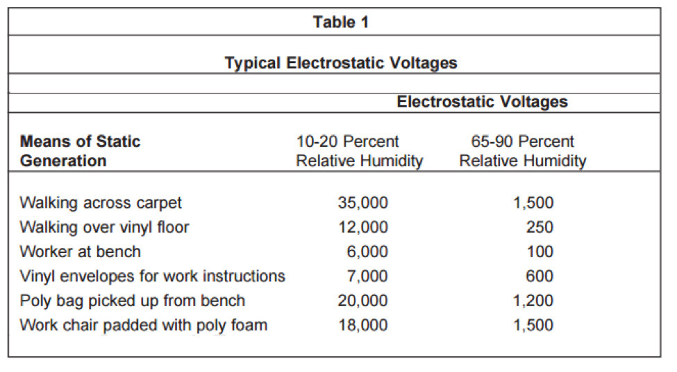
ESD damage can occur at much lower voltages than a person can detect, as the minimum ESD voltage that can be detected by a person is 2,000 V! As illustrated in the chart below, that’s already much higher than some devices can withstand.

Click to enlarge
Click to enlarge
For electronic devices, ESD causes three types of failure modes:
- Catastrophic damage, where damage or failure is immediate and parts need to be replaced.
- Latent damage (no initial sign of damage) after ESD discharge, but the damaged device eventually fails or works intermittently/erratically (needing replacement).
- Functional disruption such as unexpected resets or latch ups during operation right after an ESD discharge, but can be recovered when the device is reset or power is cycled.
The susceptibility of electronics to ESD damage increases as their density increases (and the smallest transistor features size decreases). Like other highly integrated processors, the Qualcomm Snapdragon and its high-density system components, such as high capacity SDRAM and eMMC, can be particularly susceptible to ESD damage.
Various external peripheral buses on the Open-Q development kit carrier boards, such as integrated USB, SD, and audio, are designed with standard ESD protection, but this doesn’t obviate the need for careful handling procedures, especially during transport. Also, other high-speed bus connectors (such as CSI, DSI, MIPI, and high-speed BSLP serial) are susceptible to ESD damage. When employed in end-user applications such as commercial IoT devices, proper design of your product’s enclosure and customized carrier board will ensure that only protected connectors are exposed to hazard.
To prevent damage to your development board from ESD, always take the following precautions:
1. Always store and carry your development kit pbc assemblies when not in use in an electrostatic safe container or electrostatic safe bag.


2. Before removing the board from the ESD shielding bag, ensure that you are properly grounded with an ESD wrist or foot strap and that your work space has an electrostatic safe mat or work surface.

Click to enlarge
3. Unless your board is put inside a protective enclosure, it should only be handled on an ESD safe work area where the personnel are grounded. The development boards only have ESD protection build-in on the external interfaces, such as connectors, headers, and ports. Don’t handle the development board or touch components on the board without being properly grounded first.
4. Keep plastics (bags, tools, containers, etc.), polystyrene products (Styrofoam), and synthetic clothing several feet from your development board as they carry sufficient electrostatic charges to damage electronic components. Only plastics and hand tools that have been specifically designed to be ESD safe can be used around ESD sensitive devices such as your development board.
Alec Ho is a design engineer on Intrinsyc‘s Snapdragon hardware team. He has over 20 years of experience in the electronics industry, specializing in telecommunications. His work with Intrinsyc and previous organizations such as VIAVI involved schematic capture, pcb layout, system verification, component sourcing, and equipment specification and calibration.